


FISCHERSCOPE® XDV®-µ PCB XL
New


Product may vary based on model or features
for maximum throughput
in its class for superior stability
for perfect sample handling
Uniquely built for demanding PCBs. Designed for maximum throughput.
Fast, precise, and reliable – this is our FISCHERSCOPE® XDV®-µ PCB XL! As the larger version of our trusted FISCHERSCOPE® X-RAY XDV®-µ PCB, the powerful instrument allows you to efficiently master your large-scale PCB applications, delivering market-leading accuracy. Equipped with the largest measurement area in its class, an in-house produced polycapillary optic, a large silicon drift detector, and the microfocus tube Ultra, it features everything you need to achieve high-throughput quality control of even the finest structures and the thinnest coatings, like ENIG, ENEPIG, immersion silver, or immersion tin surfaces. Discover your measuring solution for PCB formats standard systems cannot handle!

Measure large-scale PCBs with a single system.
Largest measurement area in its class, 610 × 610 mm (24 × 24 in) enables one-time positioning
Vacuum chuck for perfect sample handling.
Even thinnest PCBs are securely held in place without repositioning (optional)
Hands-free table retraction – more than convenience.
Efficient and secure handling of large-scale PCBs during XRF measurements thanks to the foot switch
Ready for the Smart Factory.
Seamlessly integrates into automated production lines – or as a standalone device
Right measurement position – automatically.
Intelligent pattern recognition speeds up measurement routines and minimizes manual operator intervention
Market-leading measurement precision.
Accurate and reproducible measurement results over the long term
Outstanding frame design.
Robust industrial-grade components and proven long-lasting design for superior stability
Reliable IPC-compliant results.
Matches relevant IPC standards for PCB coatings, ensuring maximum process reliability and quality assurance
Measure coating thickness fast, precisely, and reliably with the new FISCHERSCOPE® XDV®-µ PCB XL.

Uniquely built for large-scale PCBs. Designed for maximum throughput.
One-time positioning with the largest measurement area in its class, 610 × 610 mm (24 × 24 in), allowing you to measure demanding PCBs with a single system. The vacuum chuck holds the thinnest PCBs securely in place (optional).
Using the foot switch, the table can be retracted hands-free, enabling secure and efficient handling of large-scale PCBs during your XRF measurements.
Intelligent pattern recognition automatically finds the right measurement position, speeds up the process, and minimizes manual operator intervention.
Robust industrial-grade components for superior stability and proven long-lasting design.
Features

Microfocus tube Ultra with tungsten anode for even higher performance on smallest spots; Molybdenum anode optional

4-fold changeable filters

Up to 10 mm possible height of samples

Polycapillary optics allow particularly small measurement spots with short measurement times at high excitation intensity

Measurement spot approx. Ø 10 µm or 17 µm (FWHM)

High-precision, programmable measuring table for PCBs up to 610 x 610 mm, optionally with vacuum chuck

Silicon drift detector with 20 mm² or 50 mm² for highest precision on thin films

DPP+ for highest precision even with short measuring times

Foot switch to activate stage pop-out function
Application examples
- Measuring on smallest flat components and structures on PCBs up to 610 x 610 mm (24 x 24 in)
- Analysis of very thin coatings, such as gold/palladium layers of ≤ 3 nm or 10 nm
- Automated measuring such as in quality control
- With the 10 μm polycapillary optic option: measuring with smallest measuring spot in combination with a large silicon drift detector
- With the vacuum chuck option: measuring on flexible PCBs
- Full compliance with IPC standards 4552 and 4556 (ENIG, ENEPIG), 4553A (silver) and 4554 (tin)
Do you have further applications? Then contact us!
 Application Notes
Tutorial Notes
 Tutorials
 Webinars
 Brochures

Application Notes
AN088 Fast and non-destructive nickel phosphorus analysis for printed circuit boards 2.40 MB AN092 How to choose an XRF instrument 1.29 MB AN105 μ-spot measurements of tin and tin alloy coatings on PCBs 0.82 MB AN111 High-throughput quality control of the thinnest coatings and the finest structures on large-scale PCBs 3.21 MBTutorial Notes
Tutorials
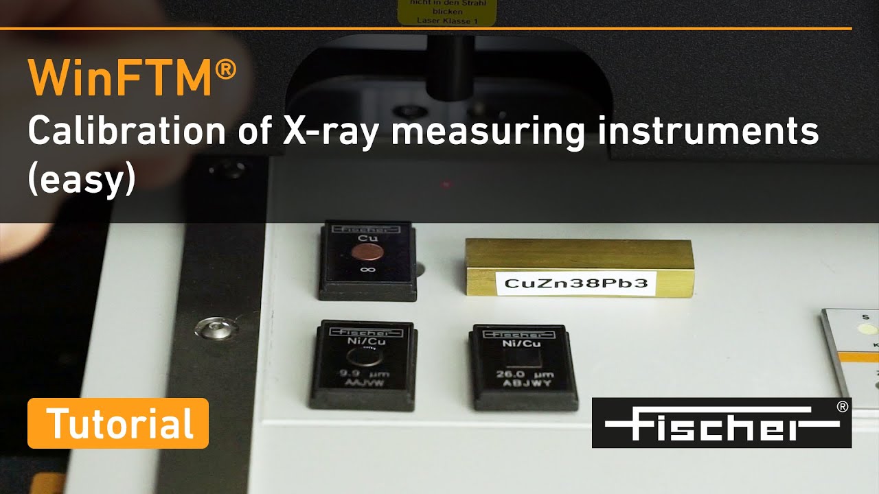
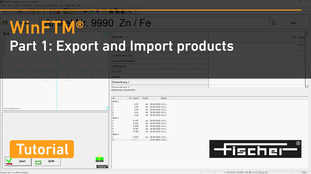
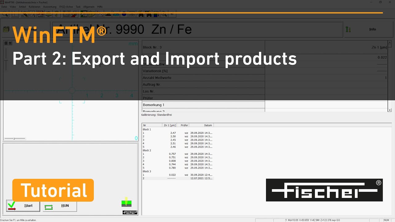
FISCHERSCOPE® X-RAY: Calibration of X-ray measuring instrumentsFISCHERSCOPE® X-RAY tutorial: Stability testFISCHERSCOPE® X-RAY tutorial part 1: Export / Import products in WinFTM®FISCHERSCOPE® X-RAY tutorial part 2: Export / Import products in WinFTM®Webinars
Setting up measurement equipment monitoringSmaller, faster and more precise: Polycapillary optics for challenging applicationsReport documentationBrochures
FISCHER insights
Discover more products


