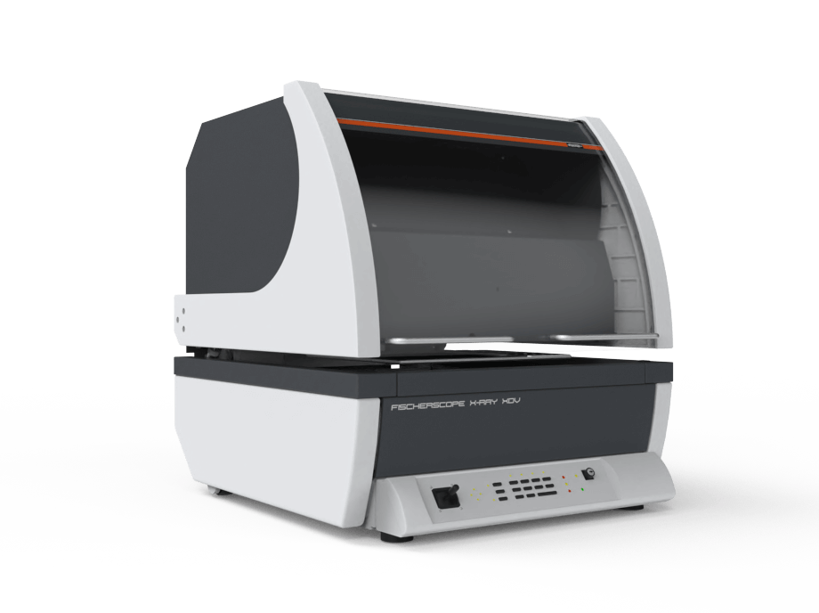
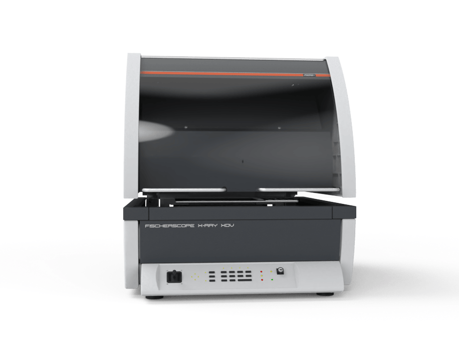
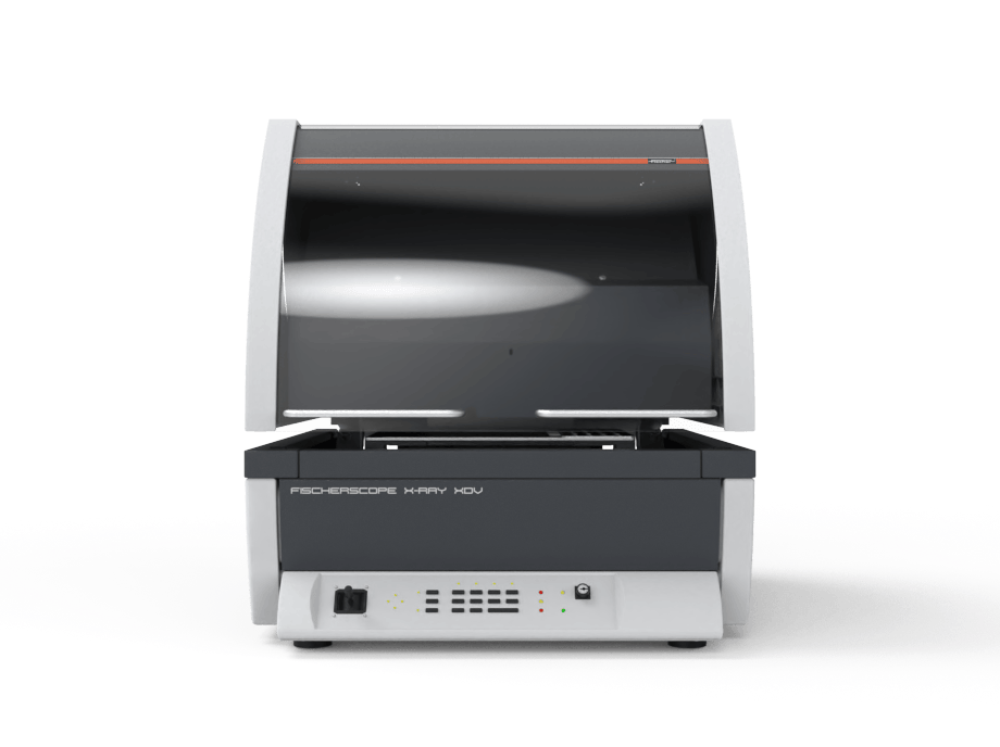
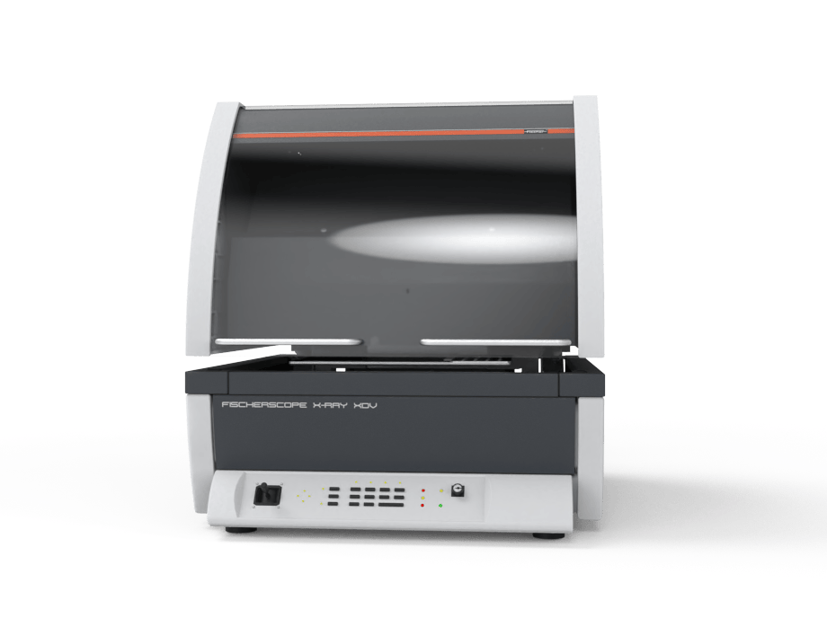
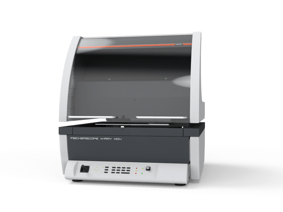
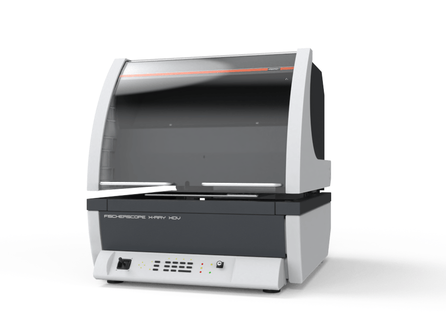
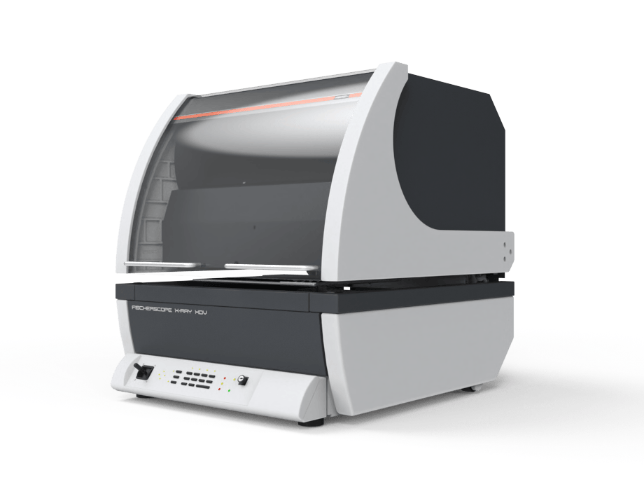
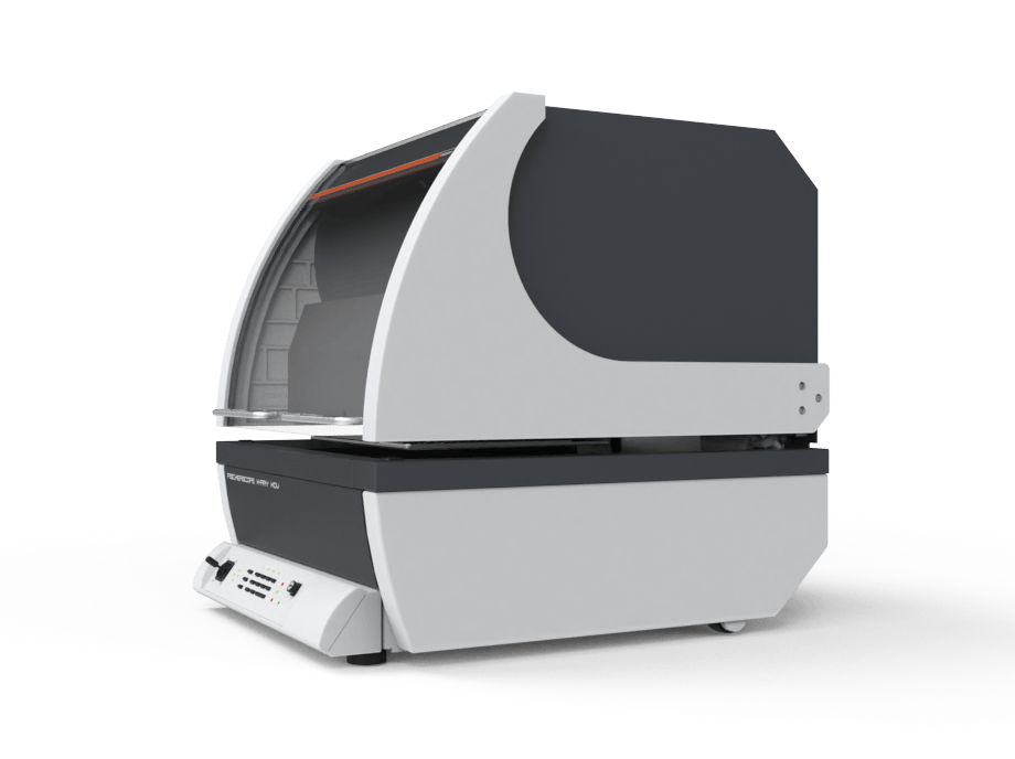
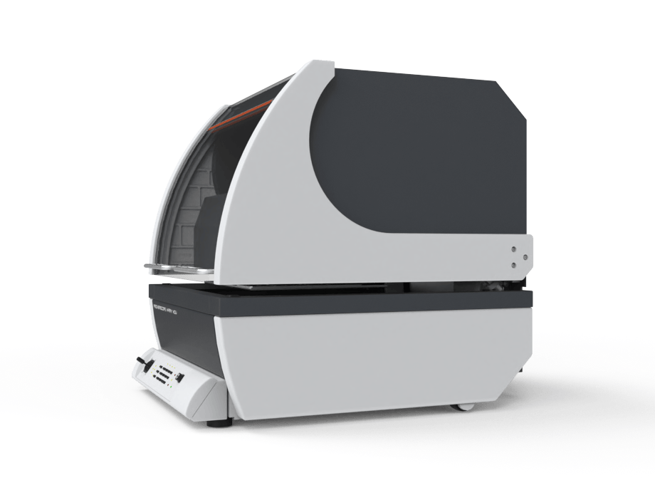
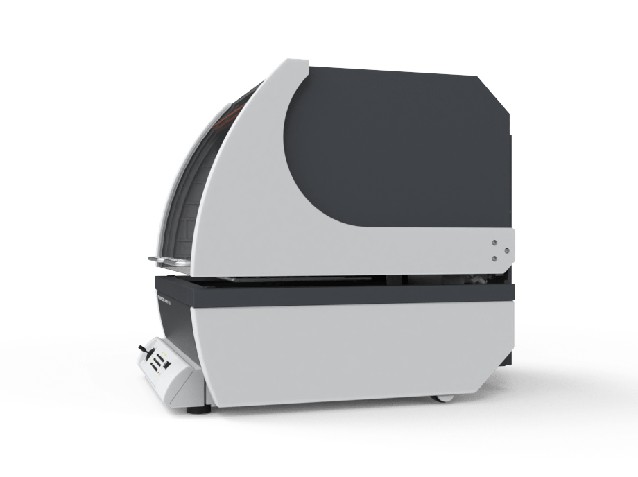
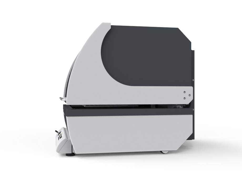
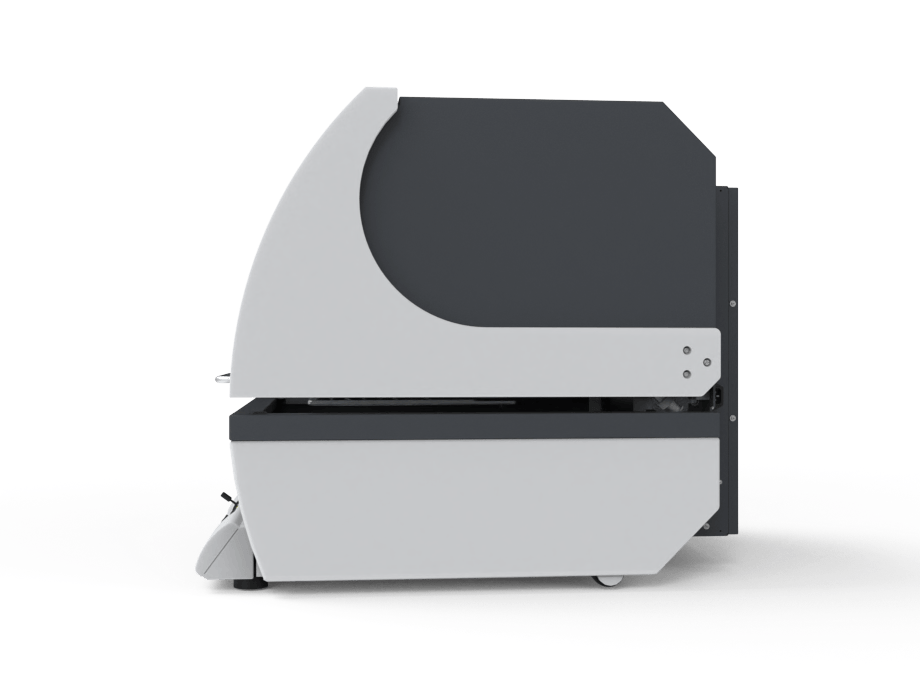
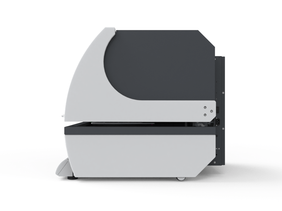
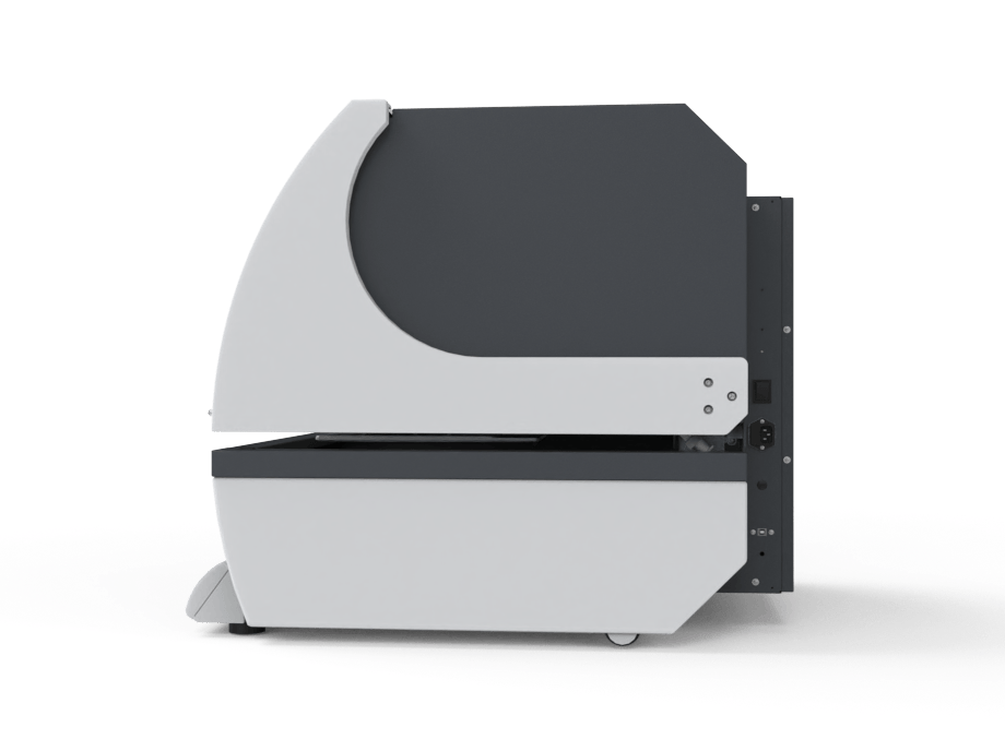
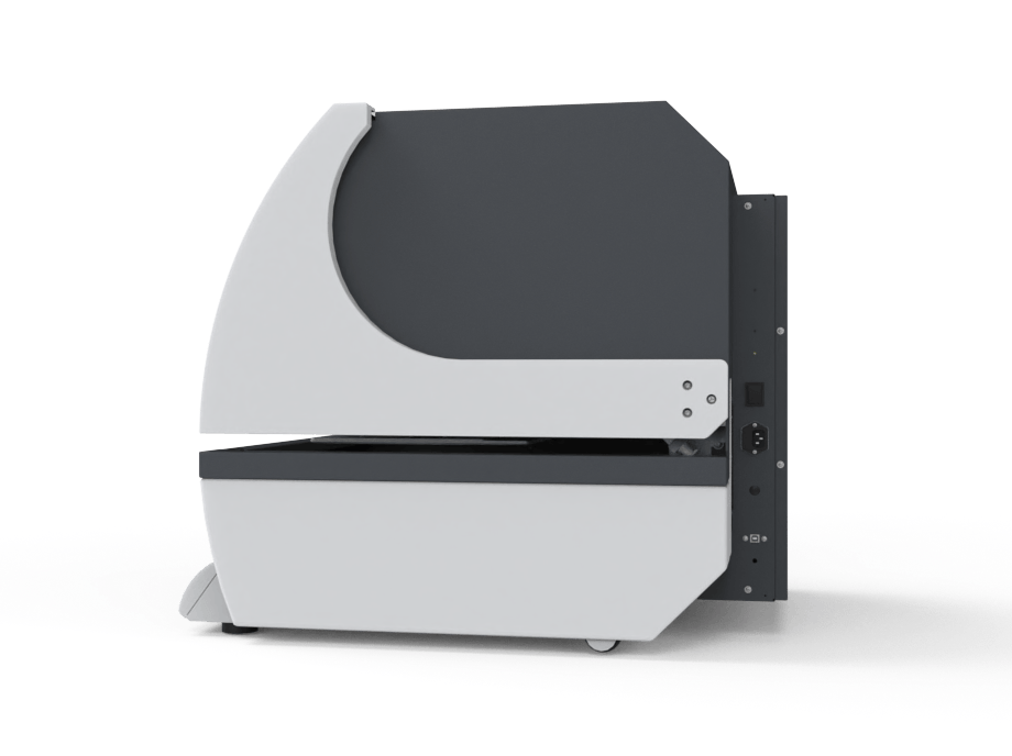
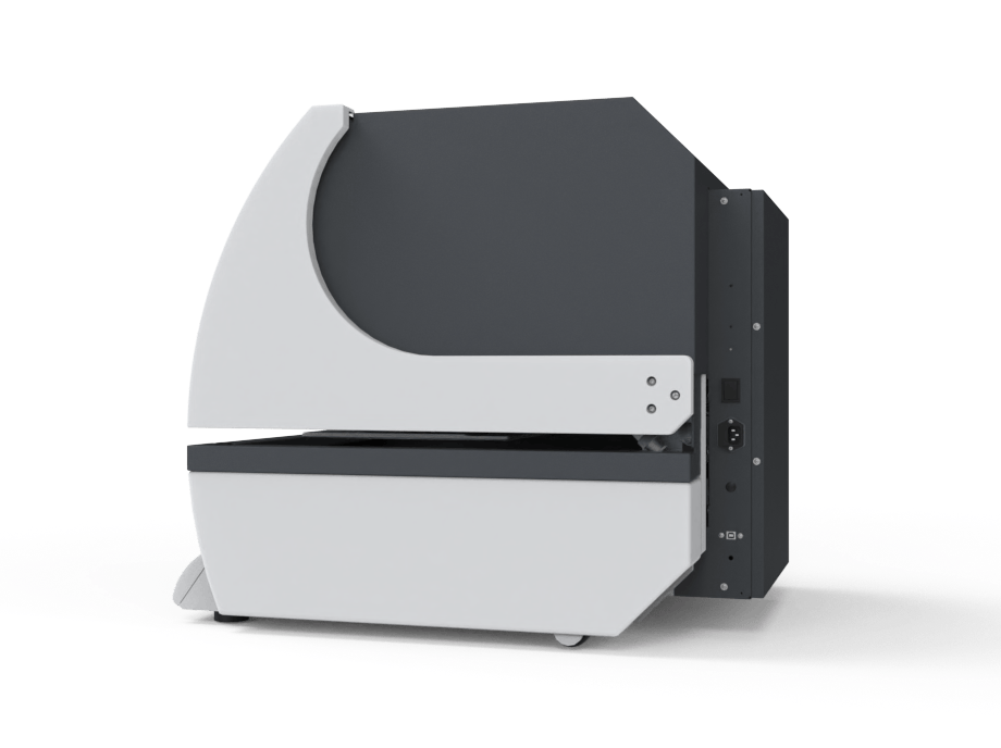
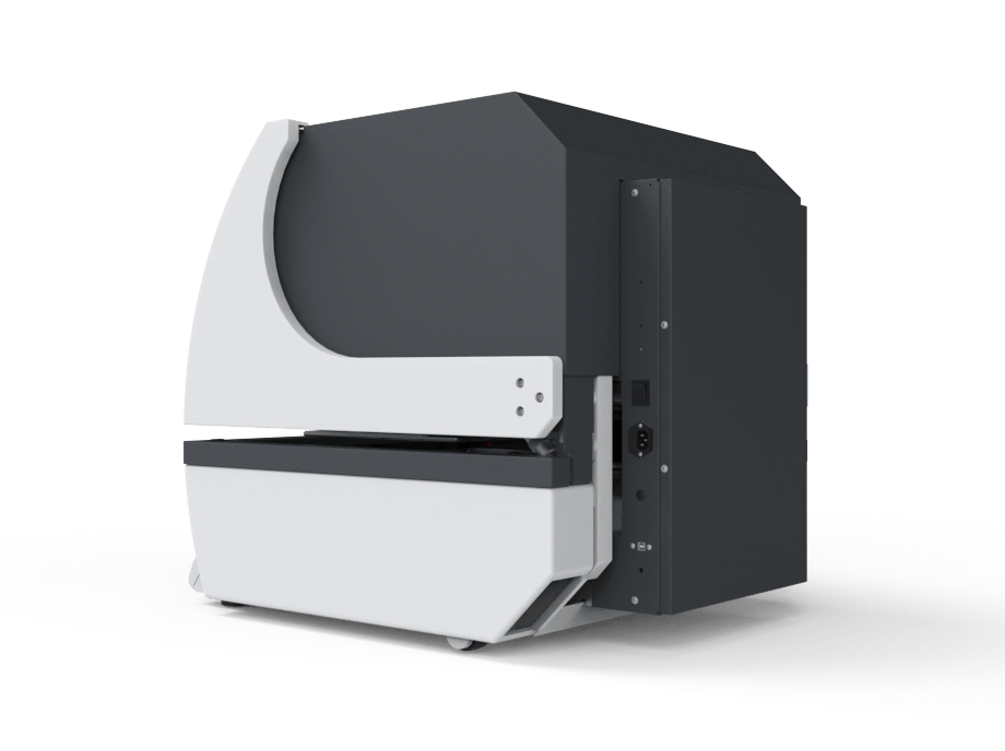
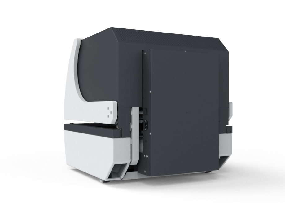
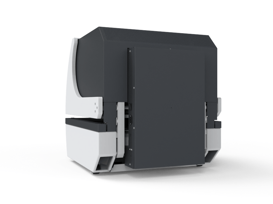
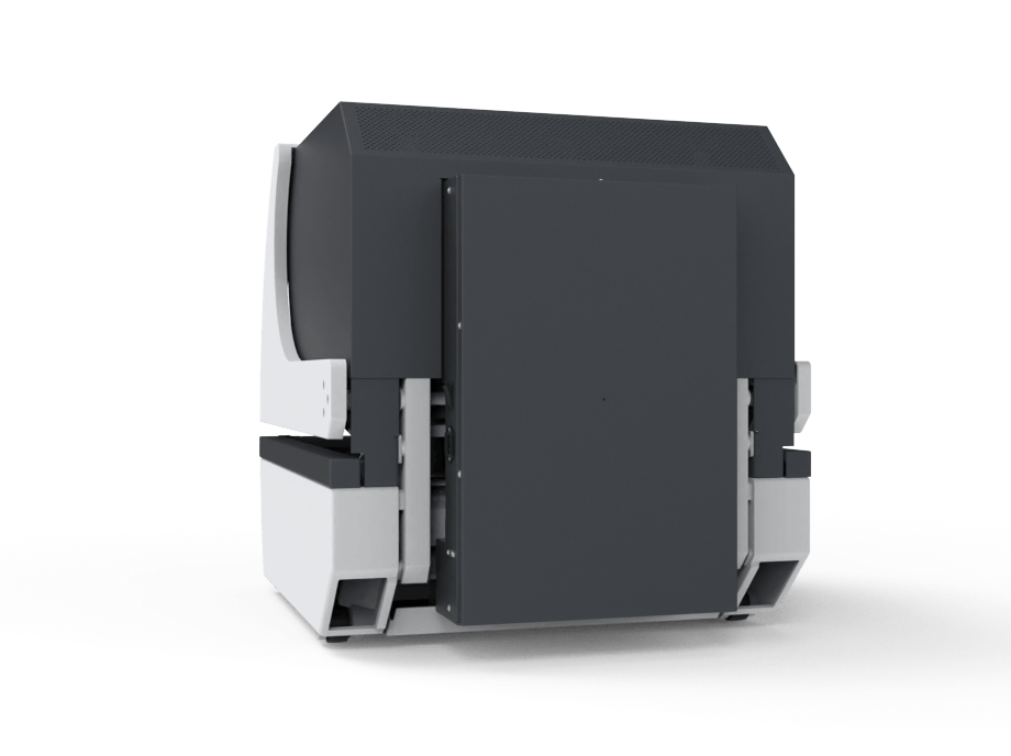
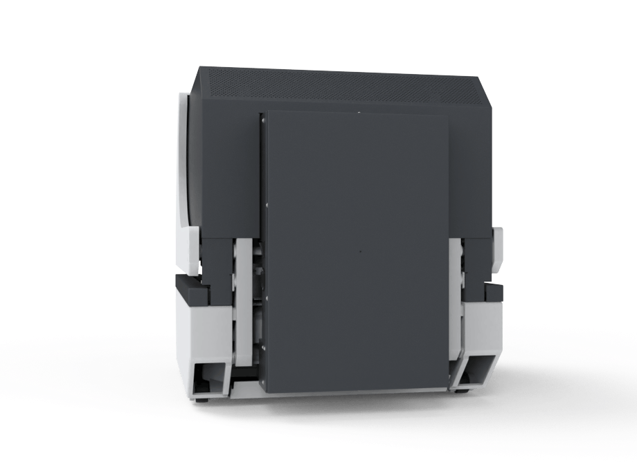
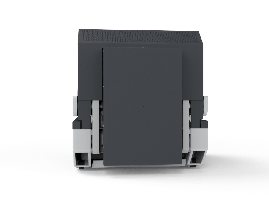
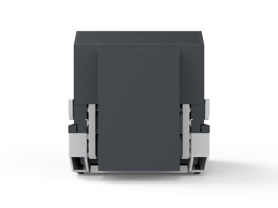
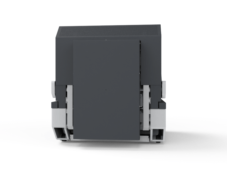
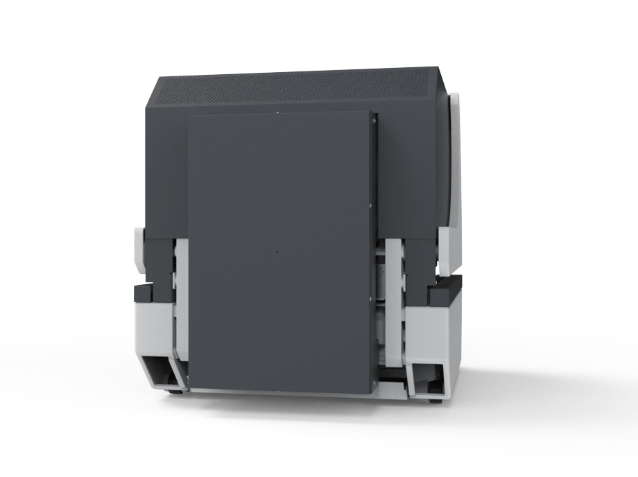
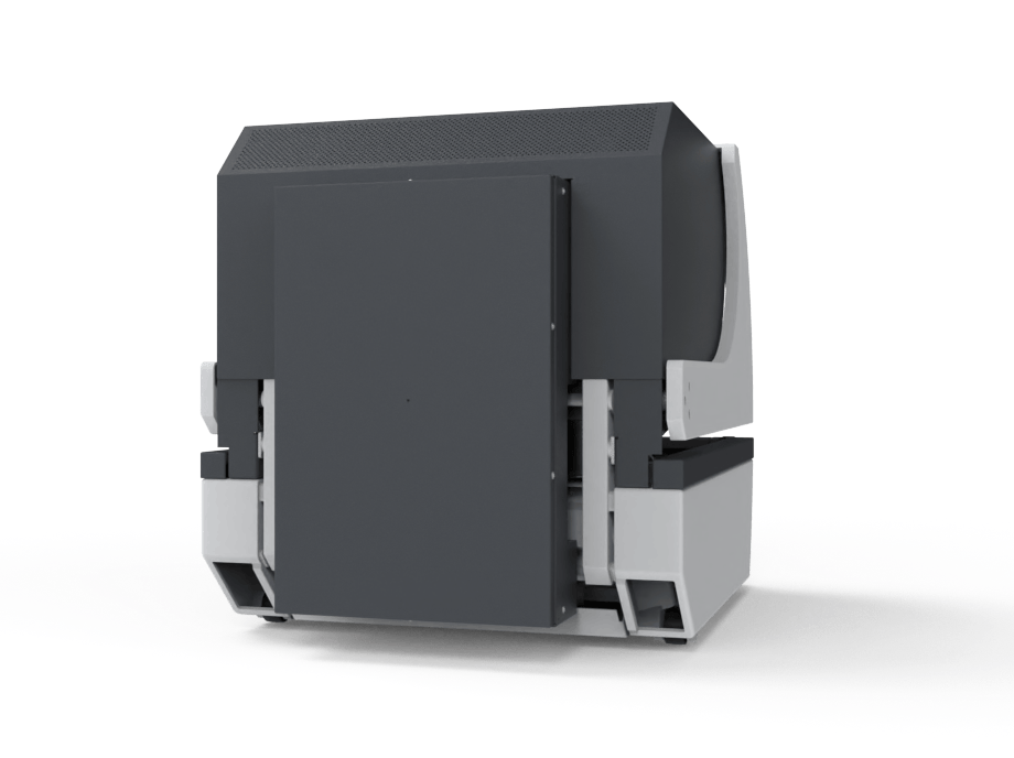
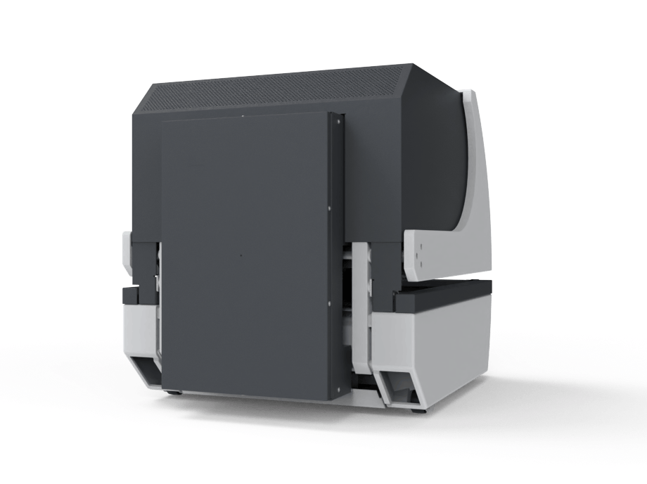
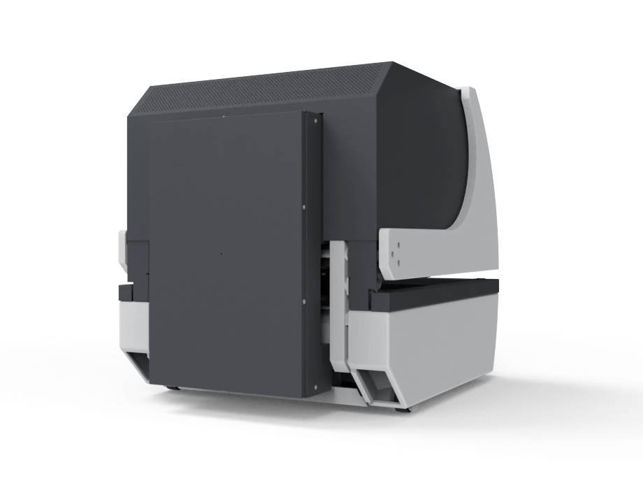
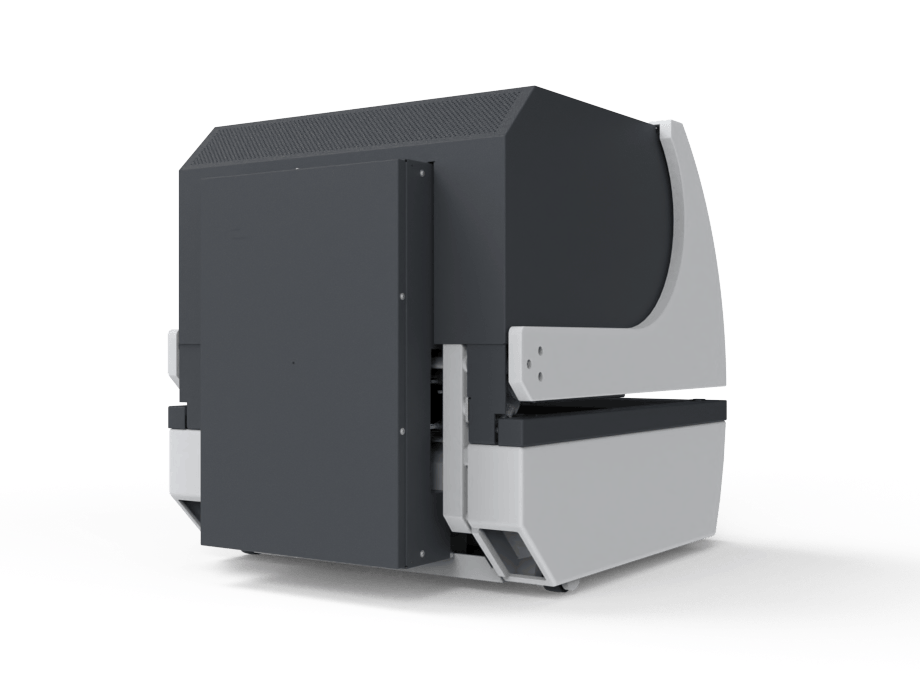
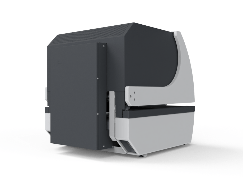
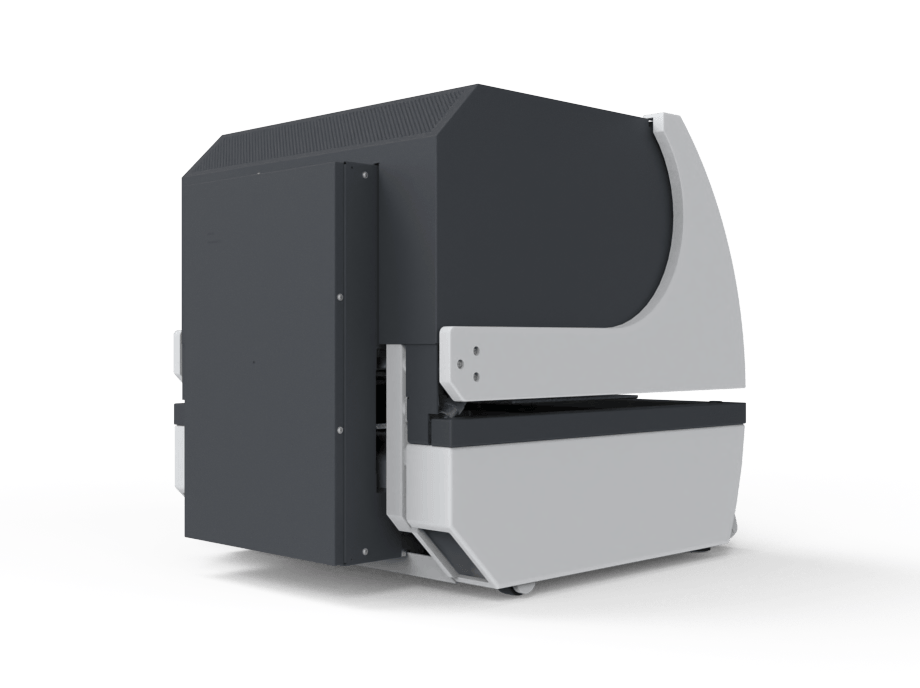
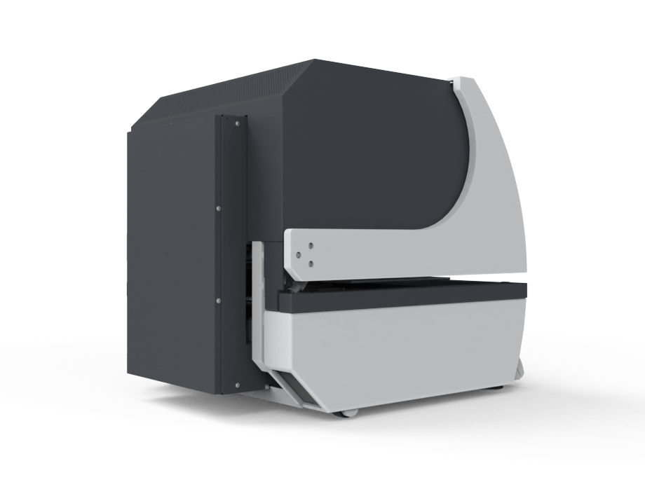
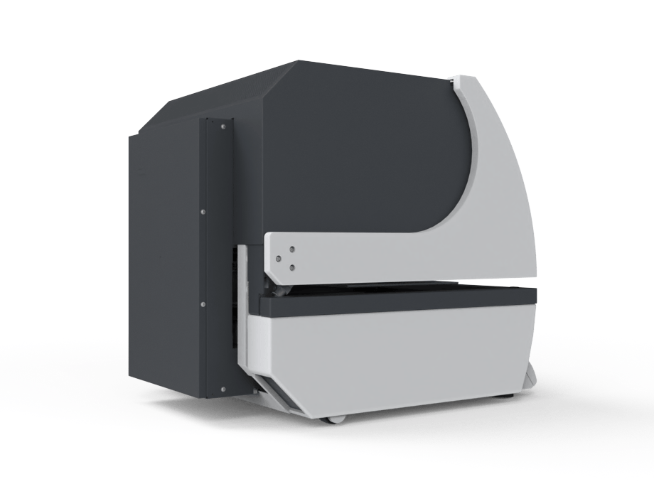
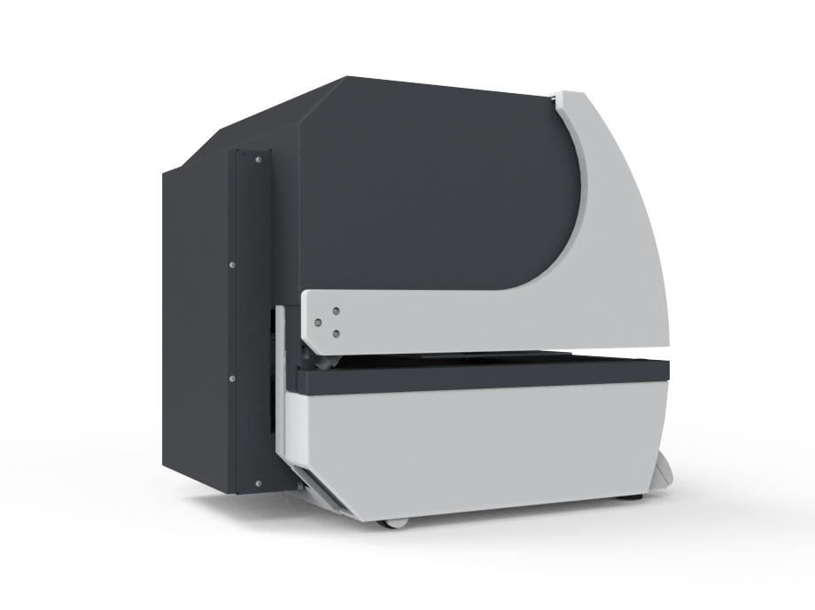
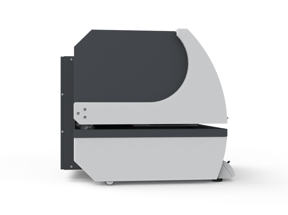
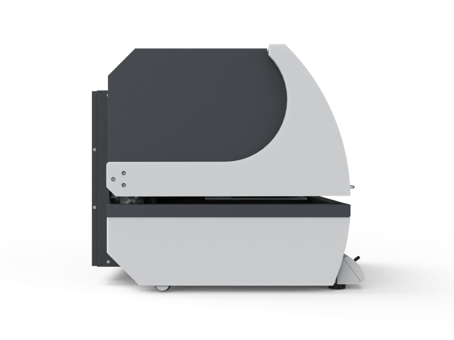
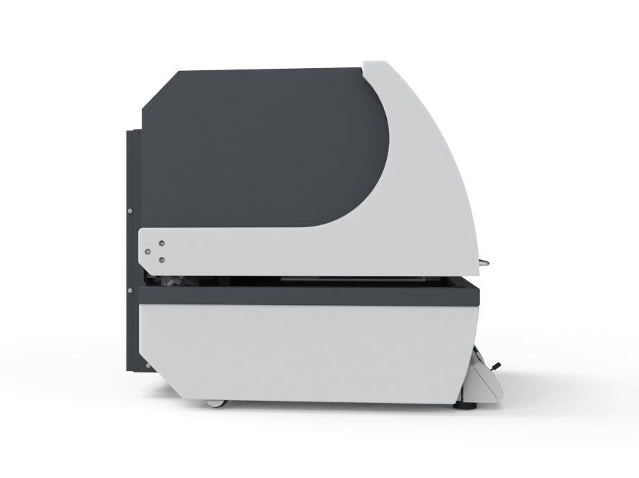
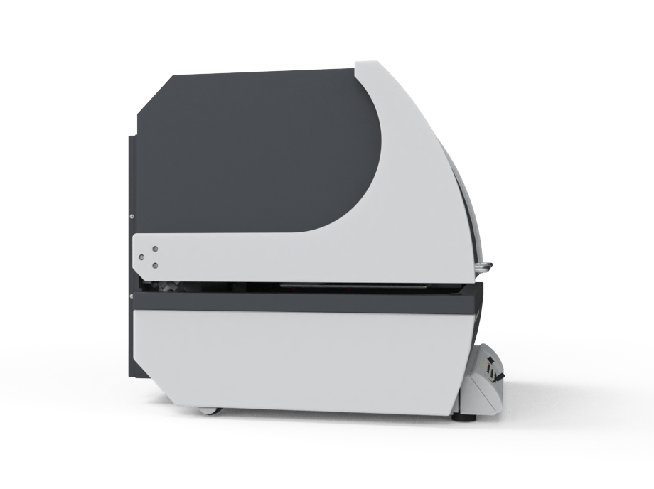
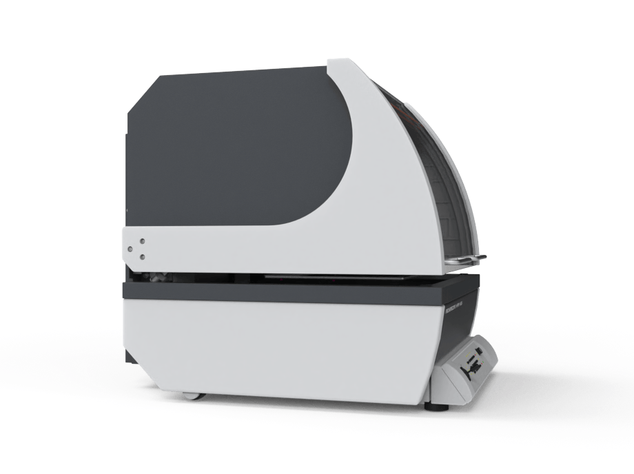
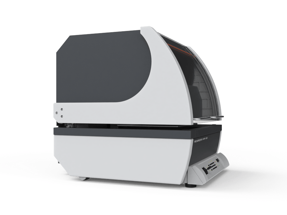
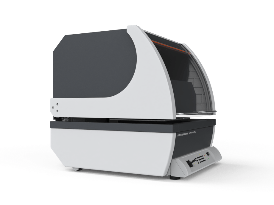
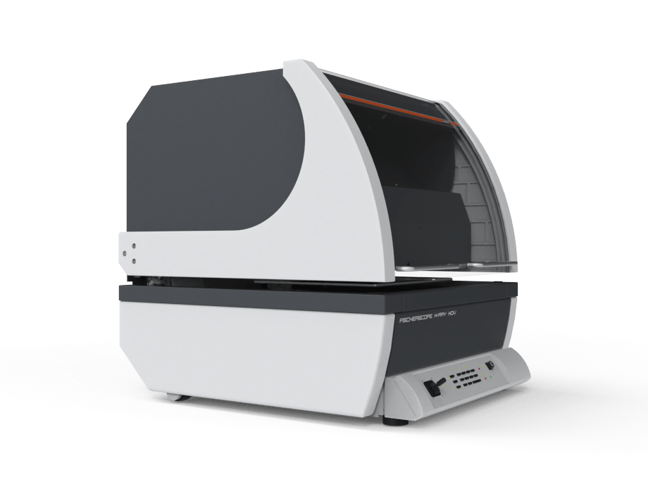
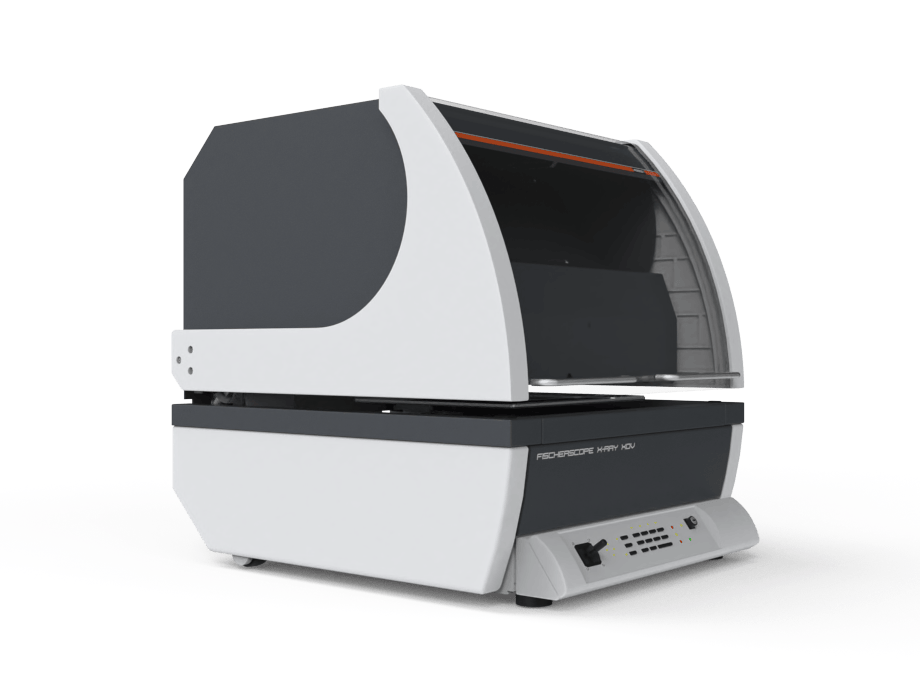
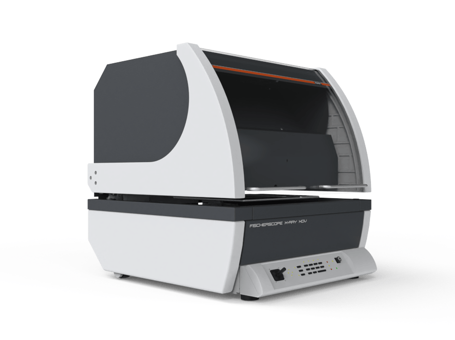
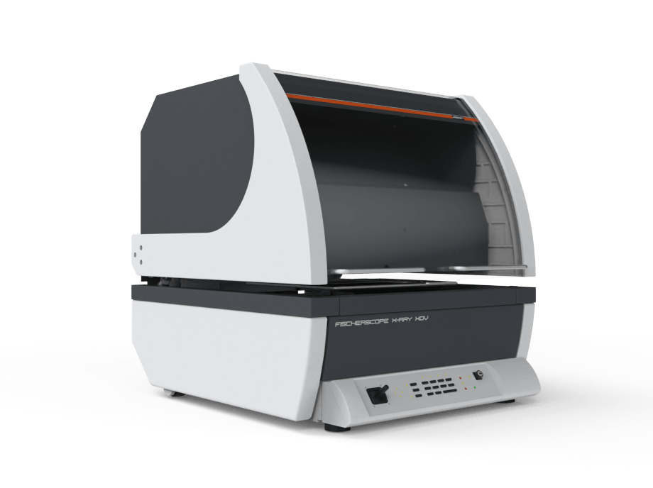
FISCHERSCOPE® X-RAY XDV®-µ

performance thanks to DPP+
Produced in-house & constantly developed²
suitable polycapillary optic³
¹ Significantly improved standard deviation and thus gauge capability or significantly reduced measurement time compared DPP to DPP+.
² Polycapillary optics, which are constantly being further developed. High-end capillary optics made by Fischer – the world's only manufacturer of X-ray fluorescence measuring instruments with its own polycapillary production.
³ Three different high-end polycapillaries available – the right solution for each of your applications: 10 µm halo-free, 20 µm halo-free or 20 µm halo.
For the highest demands down to the smallest µ.
The FISCHERSCOPE® X-RAY XDV®-µ instruments are among Fischer's high-end X-ray fluorescence measuring devices and are ideal for measuring tiny structures. They are equipped with the latest generation of powerful silicon drift detectors, microfocus tubes Ultra and in-house produced polycapillary optics. Due to the high radiation intensity, measuring times are drastically reduced and highly precise measurements on the smallest measuring spots are possible.

Meeting all challenges.
Reliable and fast results for ambitious measurement
Most advanced polycapillary optics on the market.
Our in-house manufactured polycapillary optics deliver outstanding measurement results with short measuring times
Accurate and precise.
Positioning of the measuring point on small structures thanks to automatic image recognition
Fully automatable.
Let your instrument work for you with just one click
DPP+ digital pulse processor.
Shorter measuring times or improvement of standard deviation*
*compared to the DPP
Video system with 3-fold optical zoom and WinFTM® software – ensuring precise positioning of every sample.

With the microfocus tube Ultra, the excitation intensity is significantly increased. This ensures even better measuring performance with smallest measuring spots.
Thanks to the innovative polycapillaries X-ray optics, the instrument measures with an extremely small measuring spot, while maintaining a very high intensity.
The high-performance silicon drift detector allows you to measure the smallest structures and thinnest layers < 0.1 µm precisely and non-destructive.
Features

Microfocus tube Ultra with tungsten anode for even higher performance on smallest spots with µ-XRF; Molybdenum anode optional

Changeable filter

Higher count rates and significantly reduced measurement times thanks to DPP+

Polycapillary optics allow particularly small measuring spots with short measuring times with high intensity

Measuring spot approx.: Ø 10 or 20 µm

Silicon drift detector with 20 or 50 mm² active area for highest precision

Up to 135 mm possible height of samples
Application examples
- Measuring on smallest, flat components and structures like traces, contacts or lead frames
- Measuring functional layers in the electronics and semiconductor industry
- Determination of complex multilayer systems
- Automated measuring, such as in quality control
- Measuring of light elements, e.g. determination of phosphorus content in electroless nickel under gold and palladium (ENIG/ENEPIG)
Do you have further applications? Then contact us!

Application Notes
AN003 High repeatability precision and trueness of Au/Pd coating measurements on leadframes 0.69 MB AN008 Thickness and composition of NiP on connectors or small structures on PCBs 0.56 MB AN032 Material analysis of solder bumps in the Integrated circuit (IC) packaging industry 0.57 MB AN092 How to choose an XRF instrument 1.29 MB AN093 XRF analysis for non-destructive coating thickness measurement in the field of cold forging 0.75 MB AN098 Optimized for the electronics industry: Measuring ENIG and ENEPIG on a new level 1.46 MBProduct videos
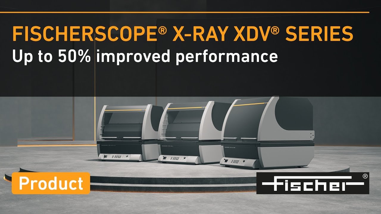
FISCHERSCOPE® X-RAY XDV® series: Up to 50% improved performanceTutorials
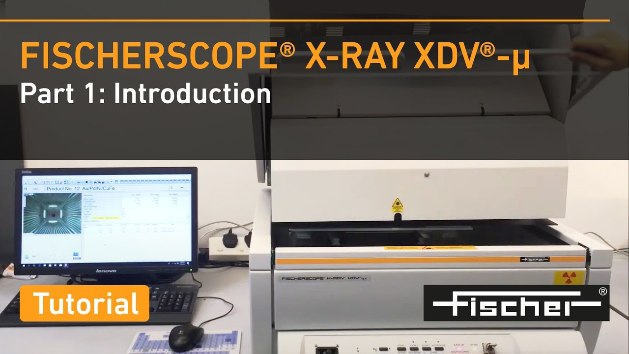
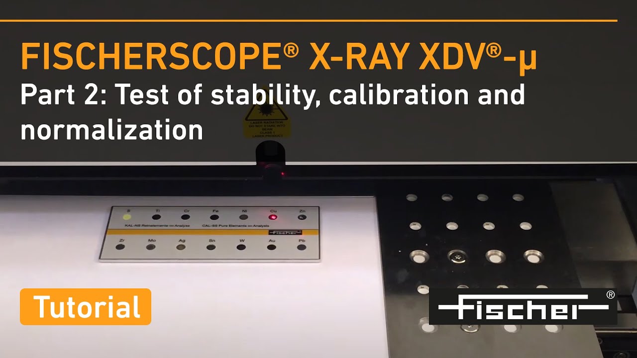
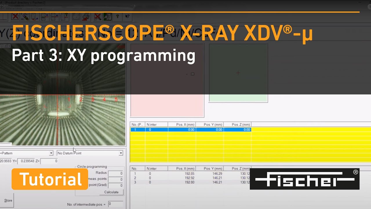
FISCHERSCOPE® X-RAY: Calibration of X-ray measuring instrumentsFISCHERSCOPE® X-RAY tutorial: Stability testFISCHERSCOPE® X-RAY tutorial part 1: Export / Import products in WinFTM®FISCHERSCOPE® X-RAY tutorial part 2: Export / Import products in WinFTM®FISCHERSCOPE® X-RAY XDV®-µ: Automated measurements on smallest structures using pattern recognitionFISCHERSCOPE® X-RAY XDV®-µ tutorial part 1: IntroductionFISCHERSCOPE® X-RAY XDV®-µ tutorial part 2: Test of stability, calibration and normalizationFISCHERSCOPE® X-RAY XDV®-µ tutorial part 3: XY programmingWebinars
Setting up measurement equipment monitoringSmaller, faster and more precise: Polycapillary optics for challenging applicationsReport documentationBrochures
Fischer Insights.
Discover more products.