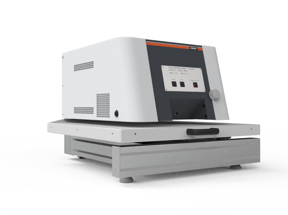
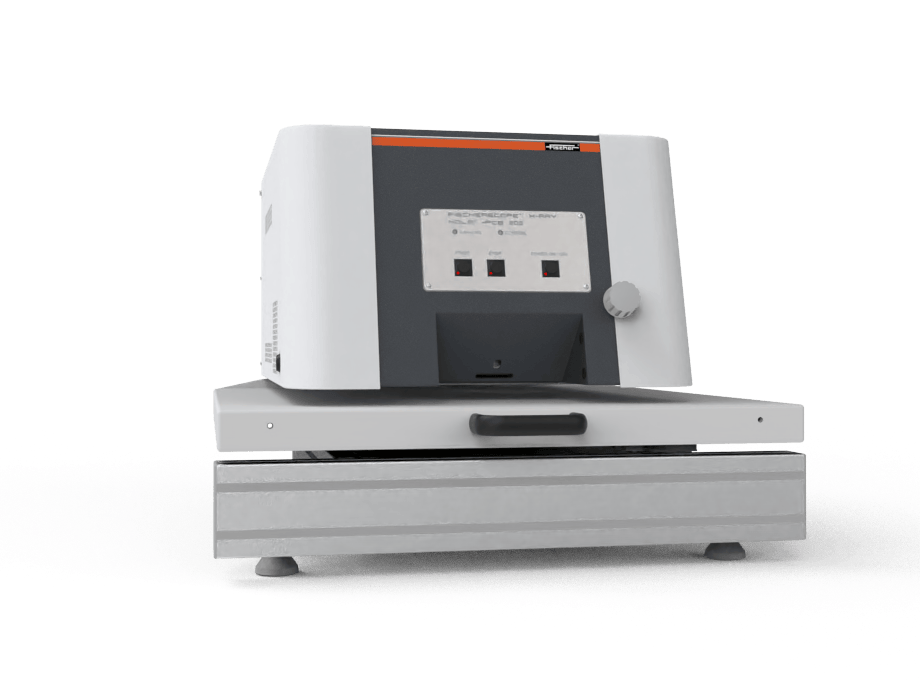
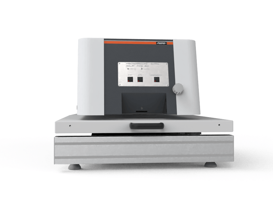
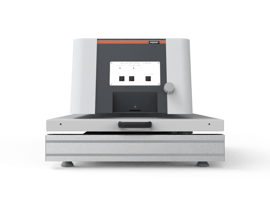
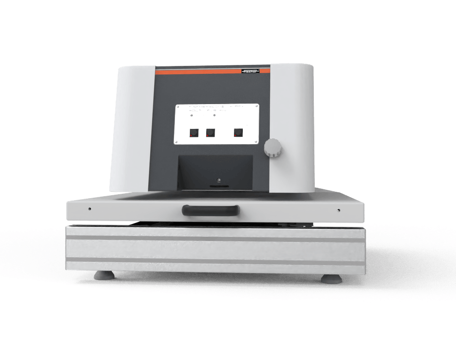
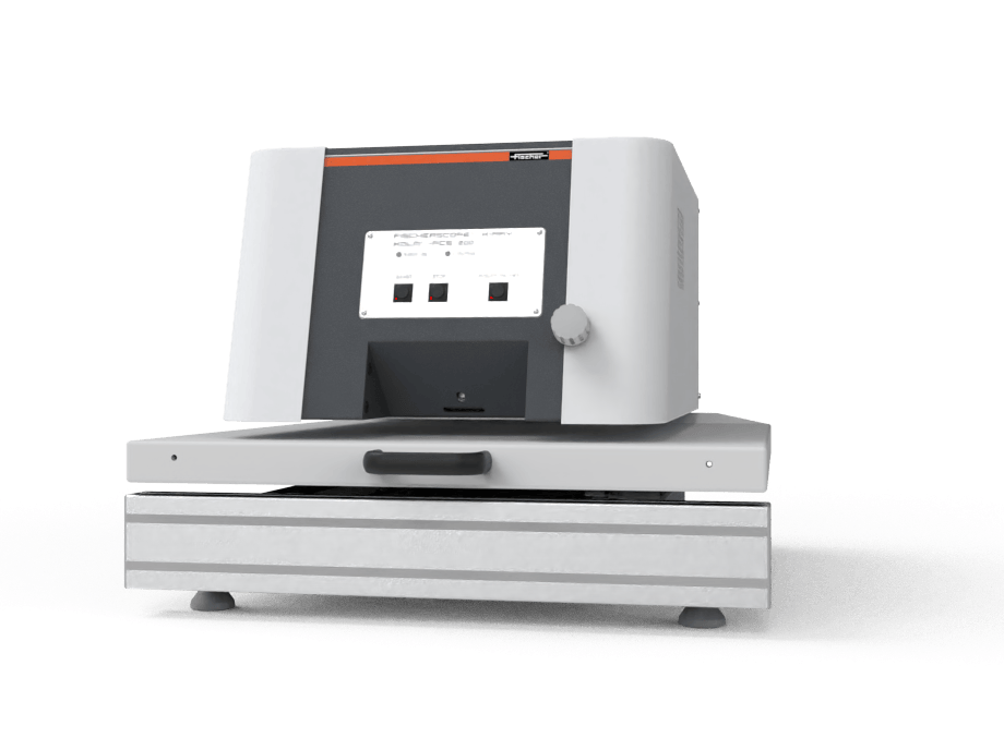
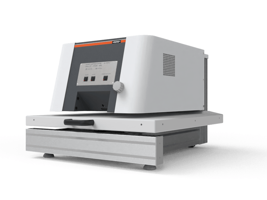
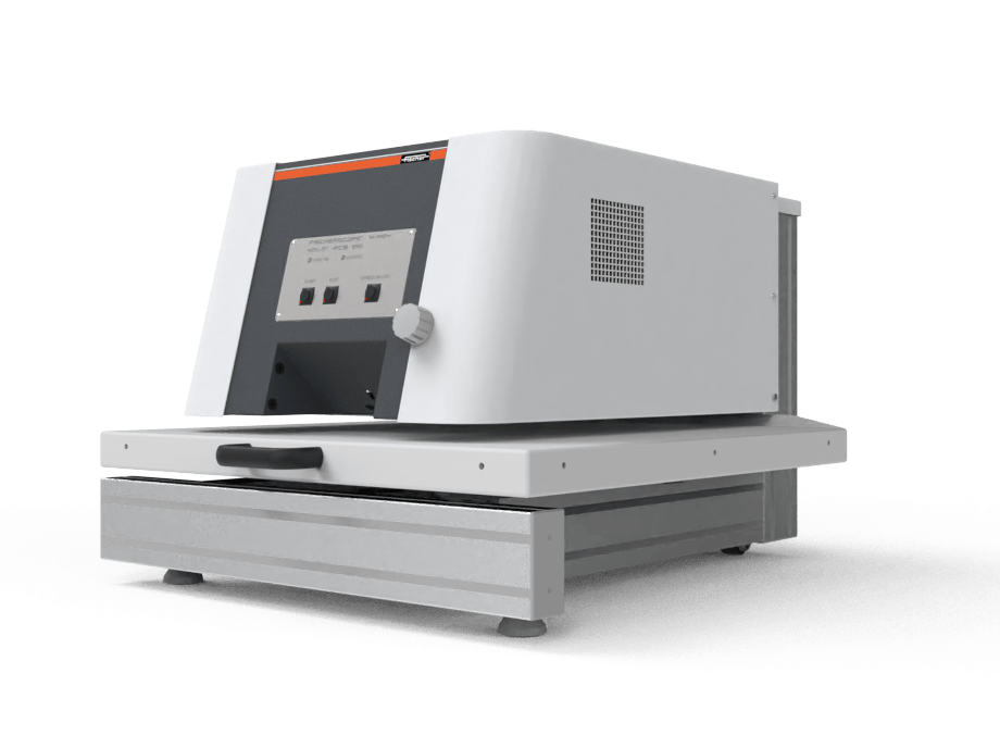
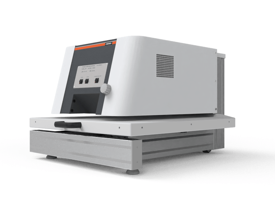
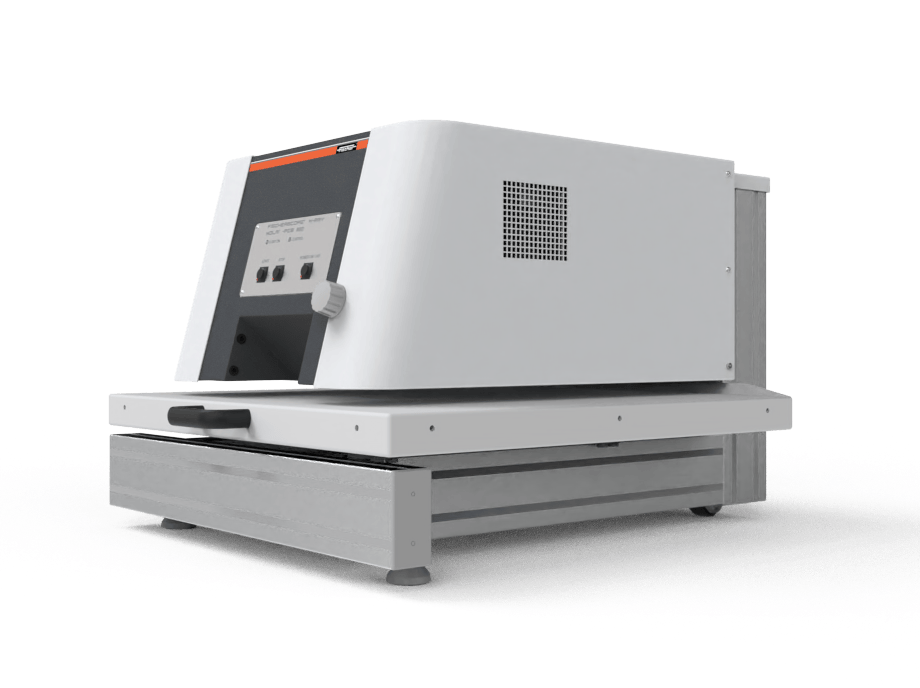
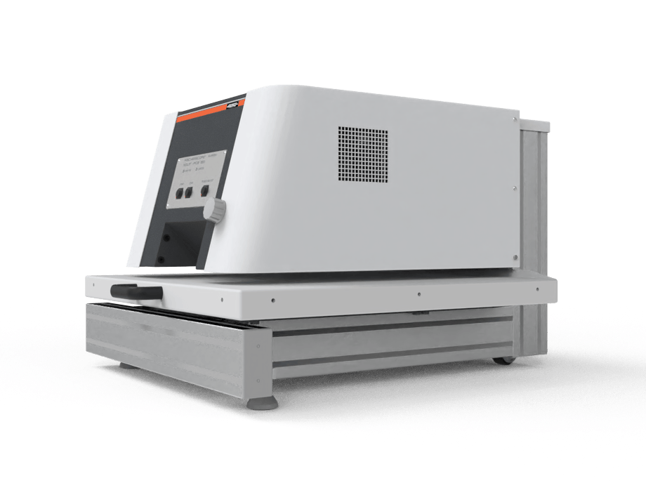
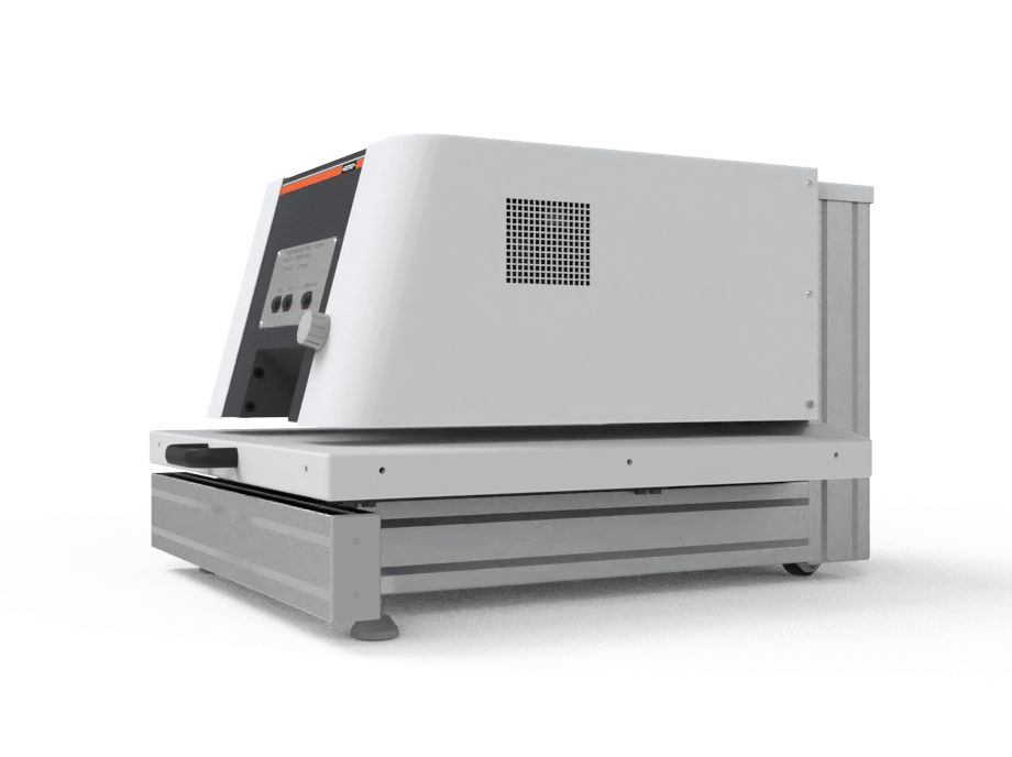
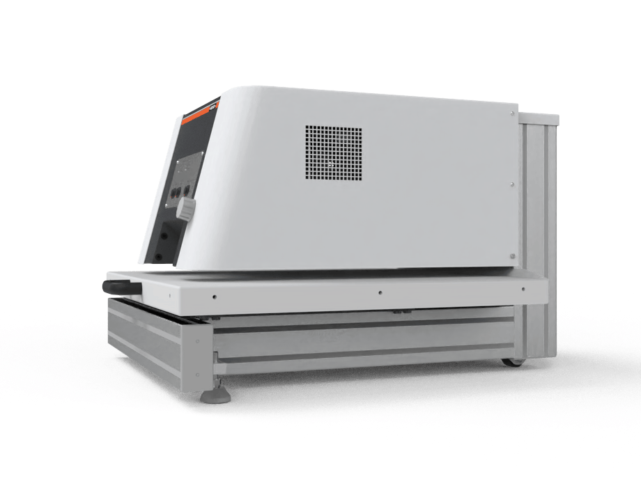
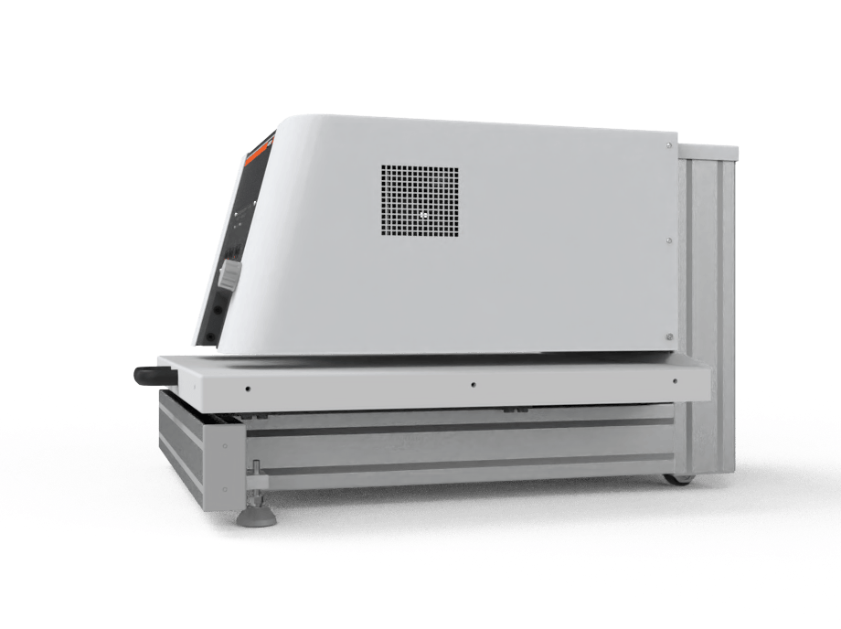
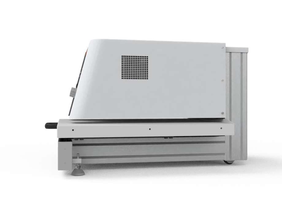
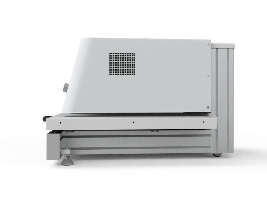
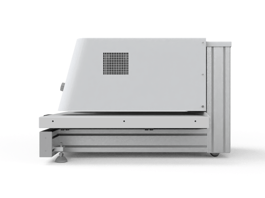
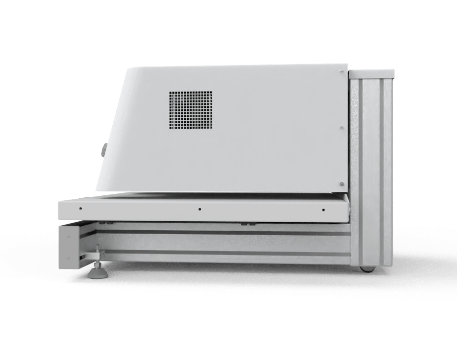
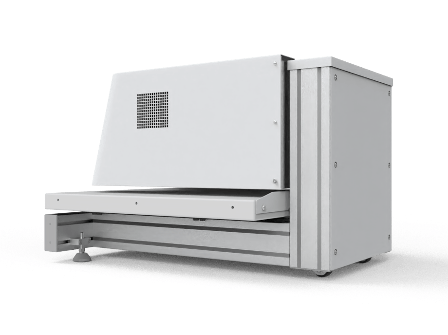
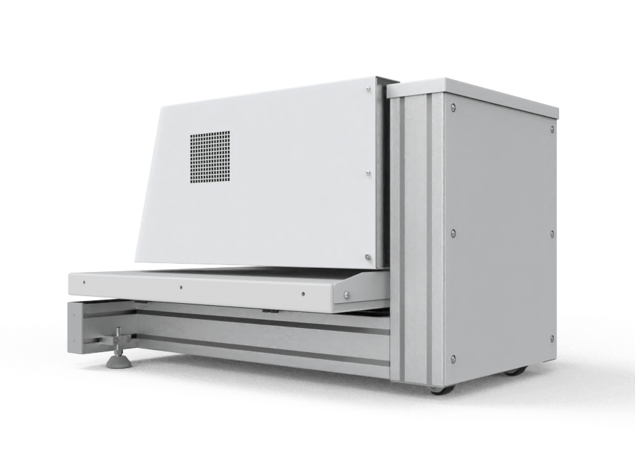
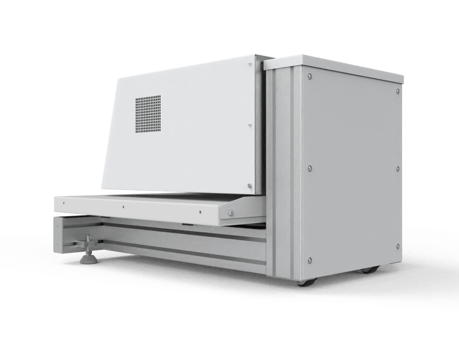
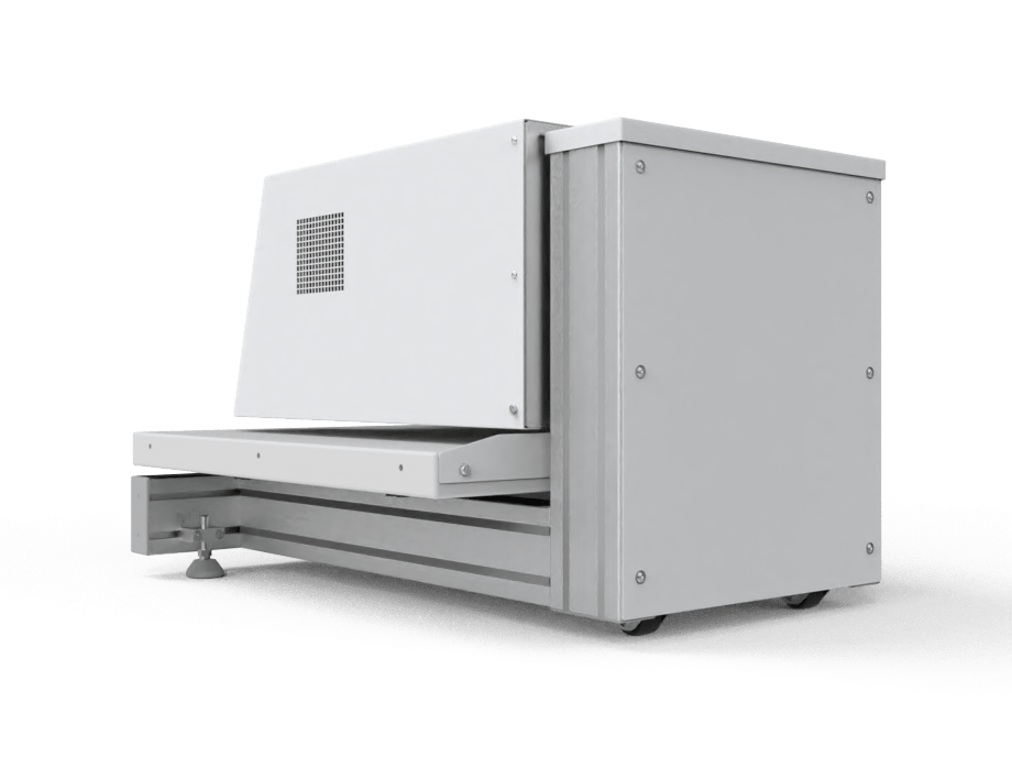
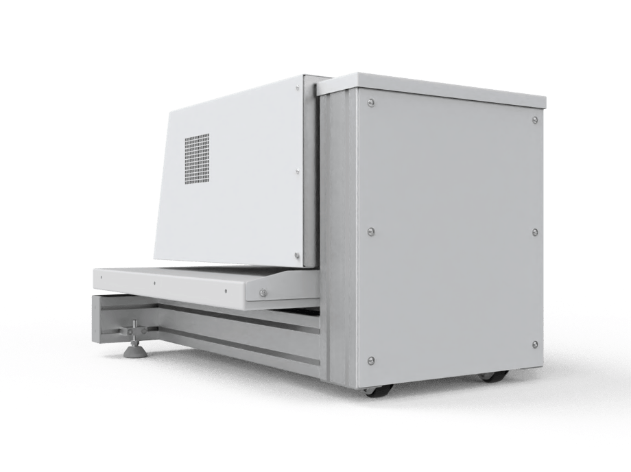
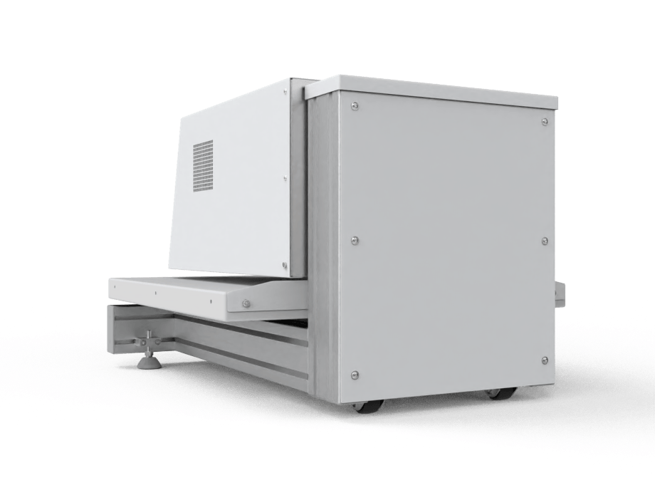
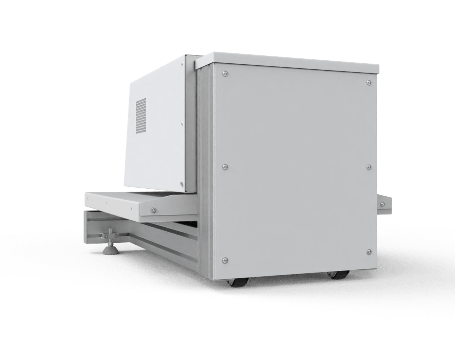
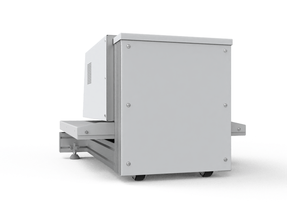
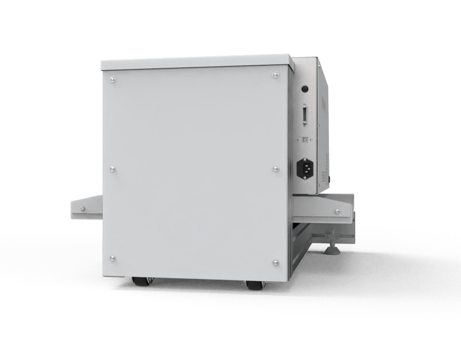
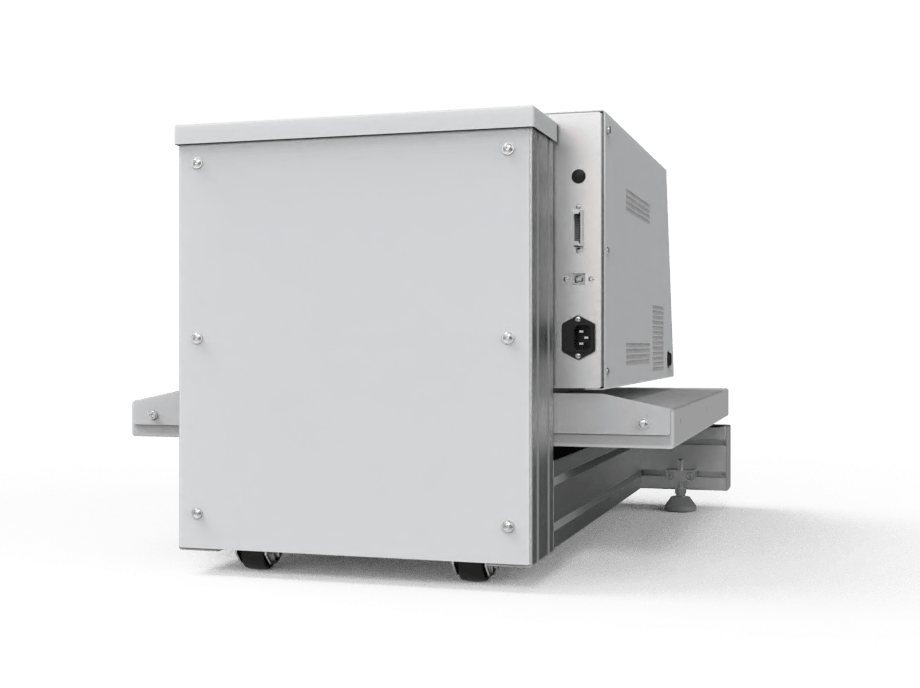
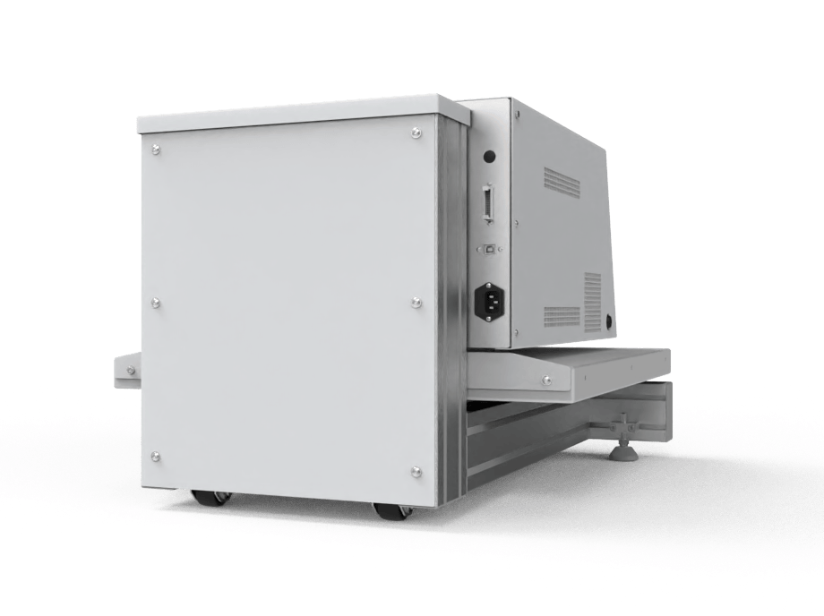
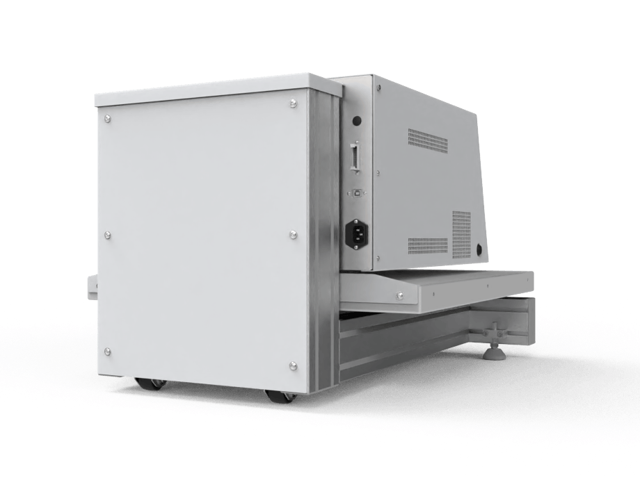
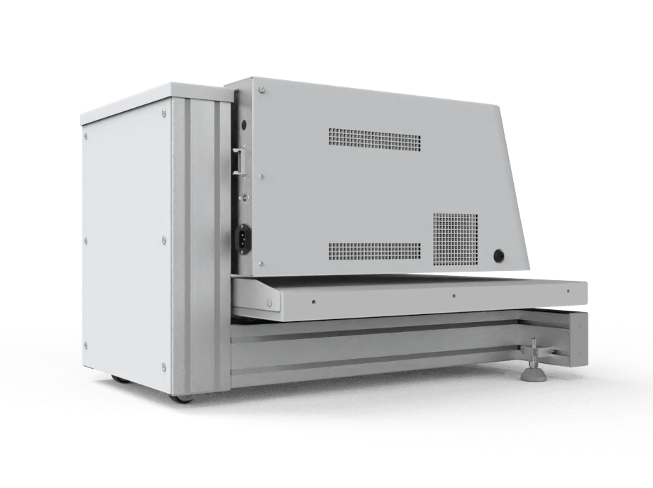
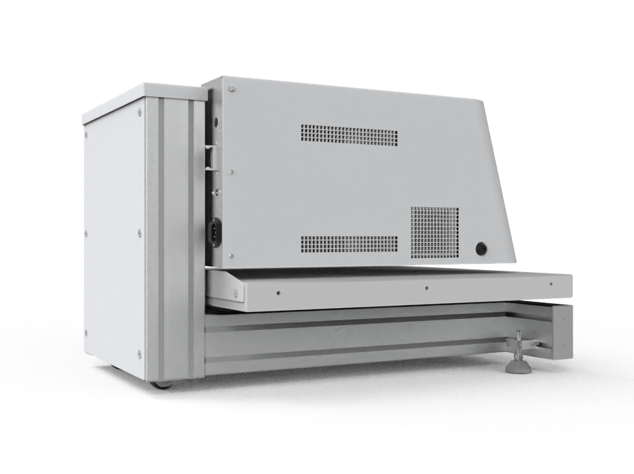
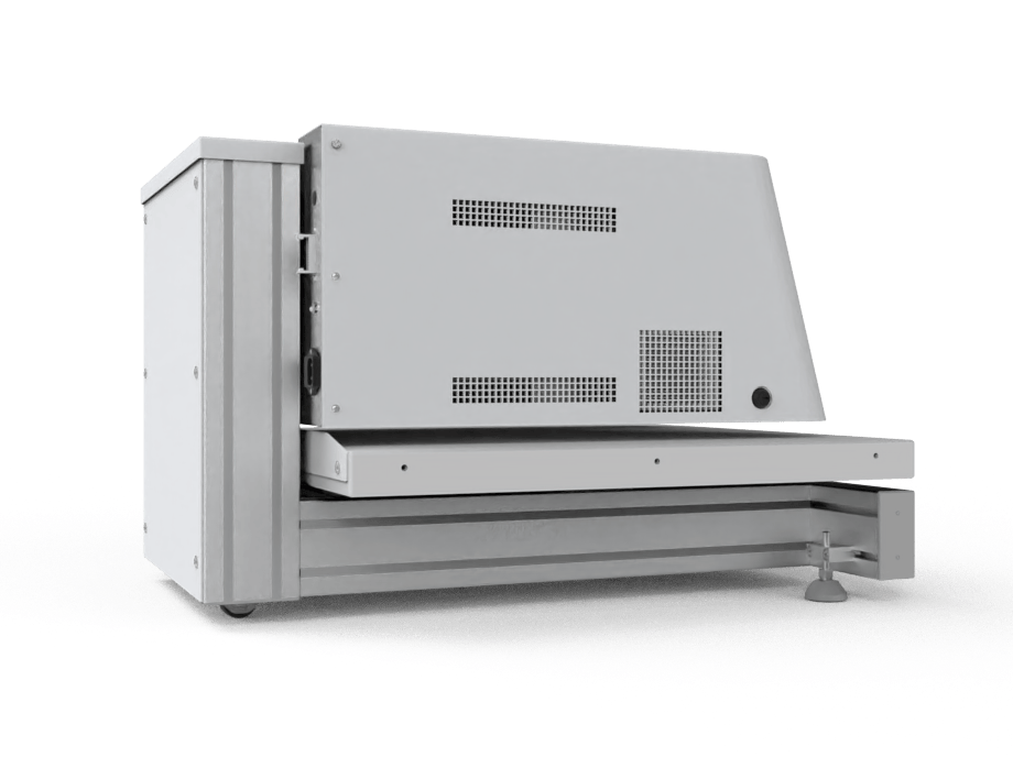
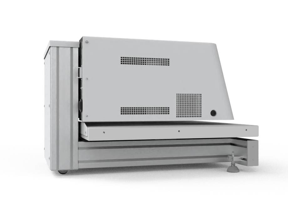
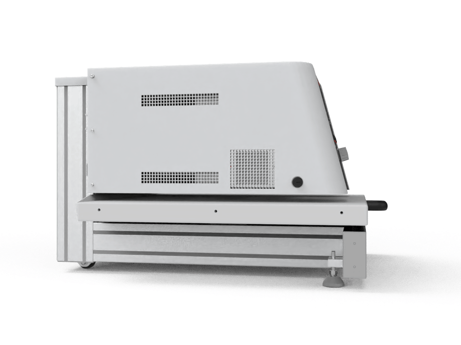
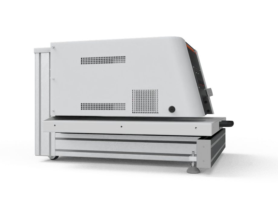
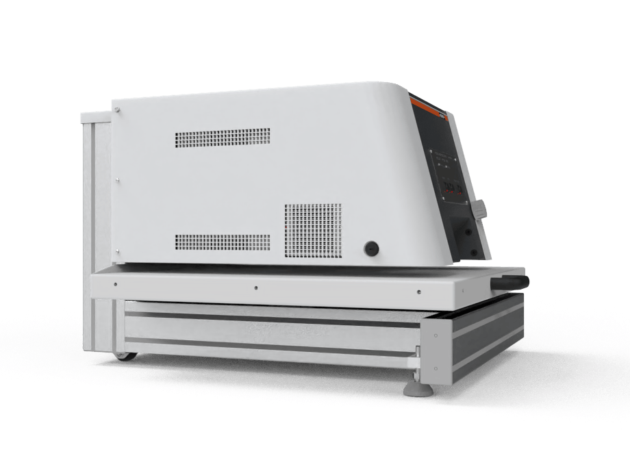
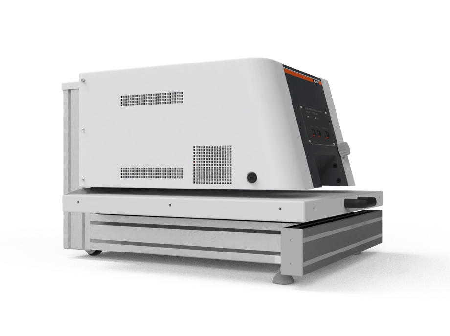
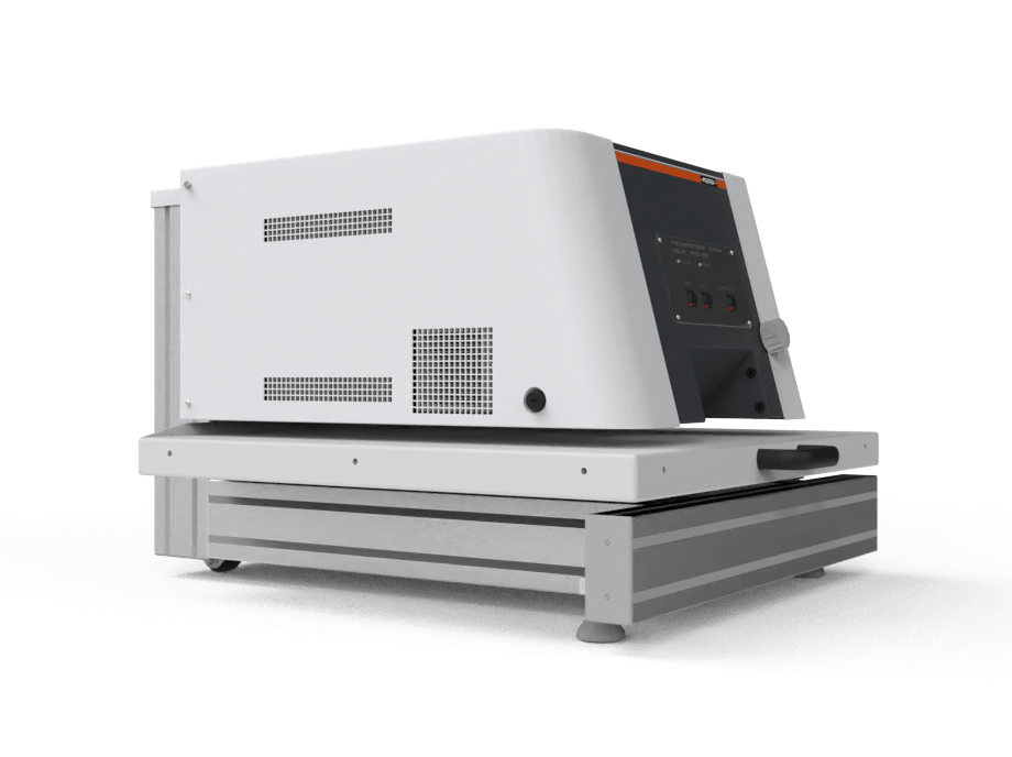
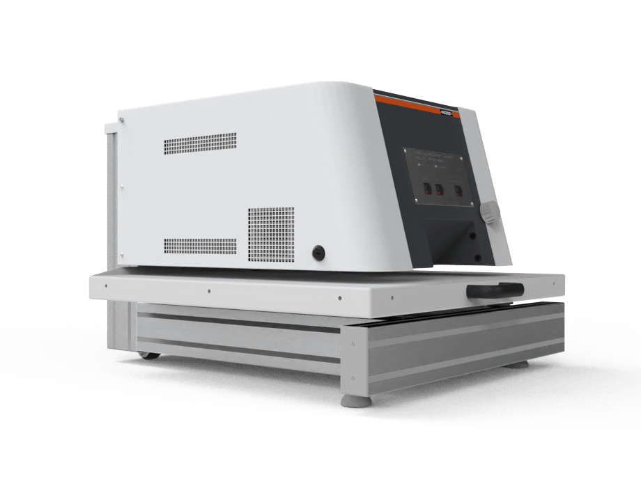
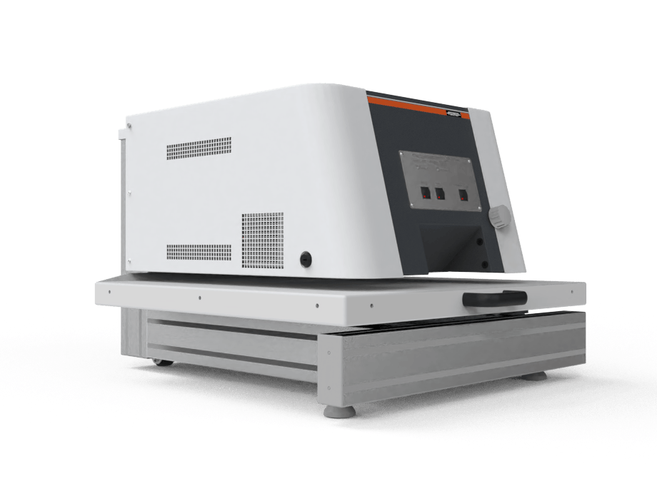
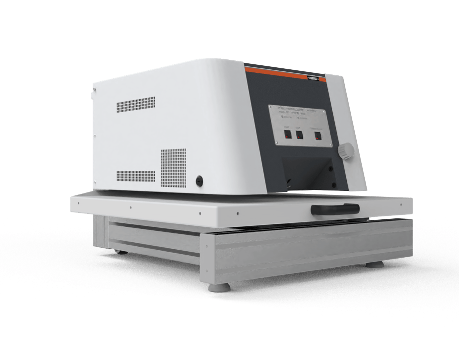
FISCHERSCOPE® X-RAY XDLM®-PCB
approx. Ø 0.2 µm
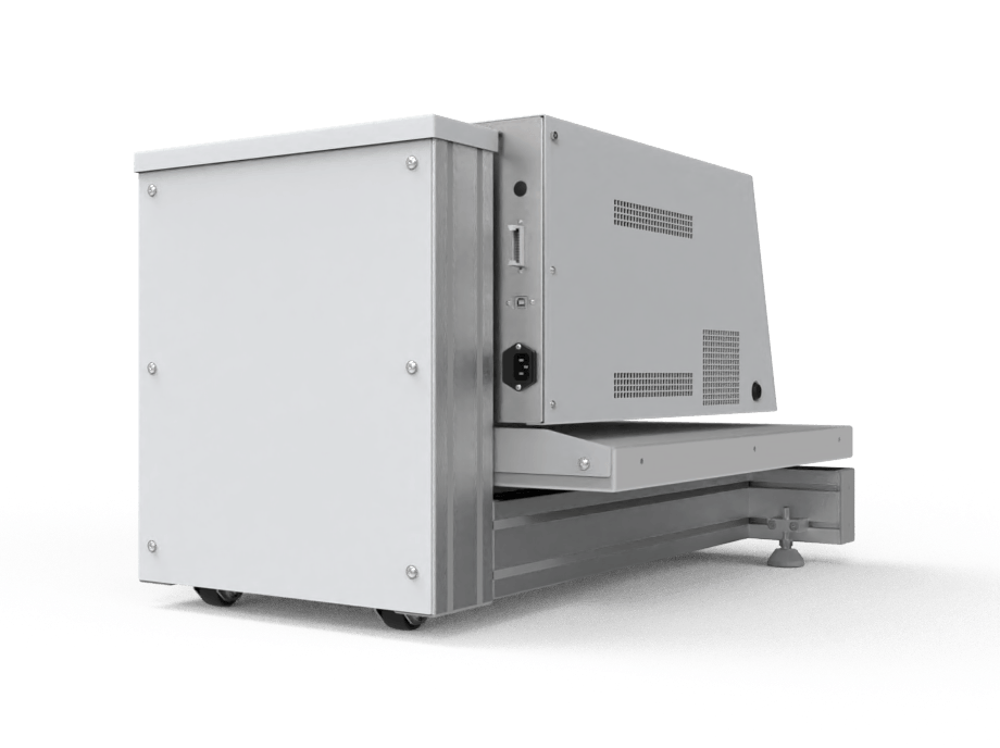
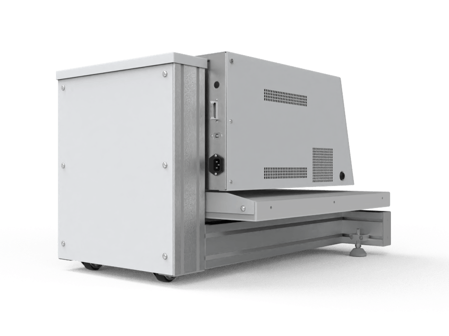
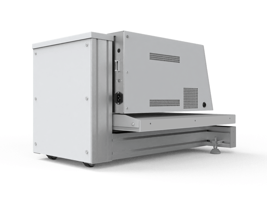
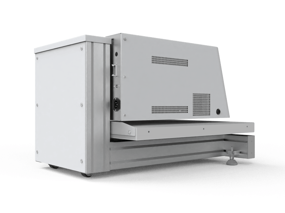
full protection device
measuring window on the market
Accurate and reliable XRF PCB inspection.
The universal entry-level instrument with a proportional counter tube detector for short measuring times is ideal for simple measurements and spot checks with a small measuring spot. Equipped with different apertures and filters, the FISCHERSCOPE® X-RAY XDLM®-PCB creates the optimal conditions for your measuring task.

Commissioning.
Extremely fast and simple
PCB experts.
Specialized measuring solutions for printed circuit boards
Accurate and precise.
Positioning of the measuring point on small structures thanks to automatic image recognition
Balanced.
Optimal cost-benefit ratio
Tailor-made.
Different models offer the optimal solution for your application
Quick-measure-design.
The sample is placed and ready for measurement in just a few steps
Real-time transmission, evaluation and export of measurement data with WinFTM®, the most powerful application software on the market.

Optional measuring table extension 1200 x 900 mm for large PCBs and a programmable XY table for automated measurements.
With the PCB instrument series, Fischer offers specialized measuring solutions for PCBs.
Accurate and precise: Positioning of the measuring point on small structures thanks to automatic image recognition.
Features

Microfocus tube with tungsten anode

Proportional counter tube detector for short measuring times and a small measuring spot

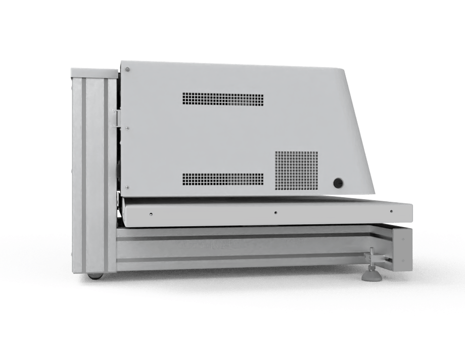
Fixed, wide measuring table for PCBs up to 610 × 610 mm, optionally with measuring table extension

Fixed aperture, optionally 4-fold changeable

Measuring spot approx.: Ø 0.2 mm

Up to 5 mm possible height of samples

Fixed filter, optionally 3-fold changeable

Measuring direction from above
Application examples
- Measuring on smallest components and structures on PCBs up to 610 x 610 mm (24 x 24 in)
- Measuring functional layers in the electronics and semiconductor industry
- XDLM®-PCB 210 and 220: Automated measuring e.g. in quality control
Do you have further applications? Then contact us!

Application Notes
Tutorials
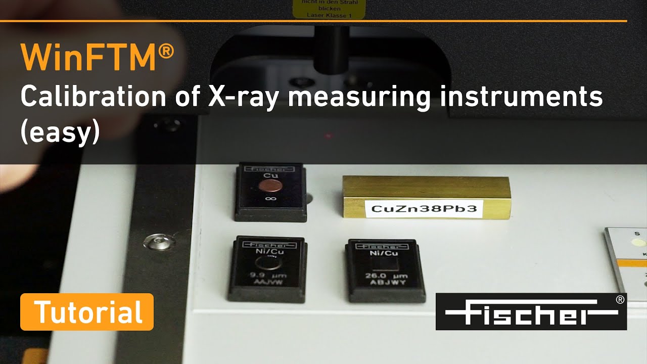
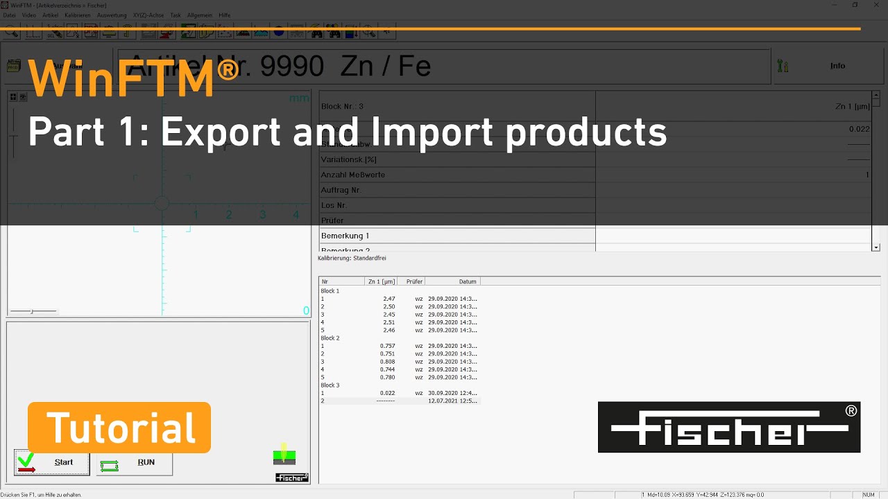
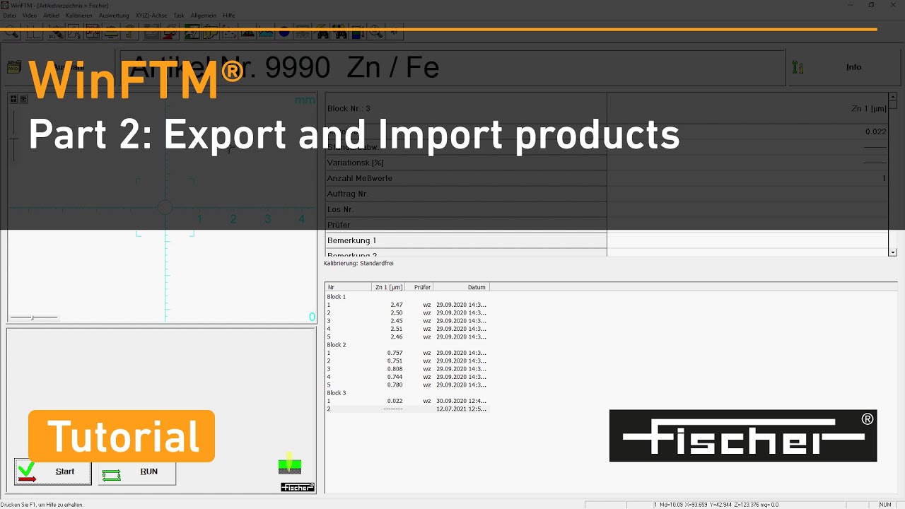
FISCHERSCOPE® X-RAY: Calibration of X-ray measuring instrumentsFISCHERSCOPE® X-RAY tutorial: Stability testFISCHERSCOPE® X-RAY tutorial part 1: Export / Import products in WinFTM®FISCHERSCOPE® X-RAY tutorial part 2: Export / Import products in WinFTM®Webinars
Setting up measurement equipment monitoringReport documentationBrochures
Fischer Insights.
Discover more products.